A igbt deep trench photolithography process

A photolithography process and deep trench technology, applied in the field of microelectronics, can solve the problems of poor and insufficient etching effect of IGBT deep trenches

Active Publication Date: 2017-12-08
ZHUZHOU CRRC TIMES SEMICON CO LTD
View PDF4 Cites 0 Cited by
  • Summary
  • Abstract
  • Description
  • Claims
  • Application Information

AI Technical Summary

Problems solved by technology

[0008] The invention solves the technical problem of poor and insufficient etching effect in the IGBT deep trench

Method used


Image

  • A igbt deep trench photolithography process
  • A igbt deep trench photolithography process
  • A igbt deep trench photolithography process

Examples


Embodiment 1

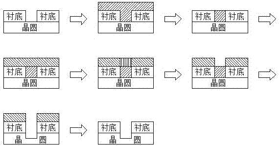
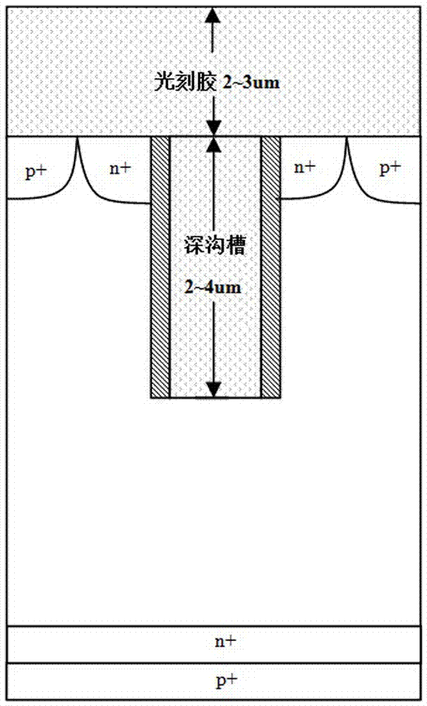
[0030] Since in the process of manufacturing IGBT devices, it is necessary to perform photolithography on the deep grooves on the device substrate, so that the wafer at the bottom of the deep grooves can be etched with a certain pattern, this embodiment provides a new deep groove photolithography method. Engraving process, pre-filling organic materials in deep trenches, other processes are all existing technologies, such as figure 1 As shown, the specific steps are as follows:

[0031] (1) Use a rotary coating machine to coat a layer of organic material on the surface of the substrate and in the deep groove at a speed of 850 rpm; the organic material is GF52 from Nissan (Nissan) in Japan. The composition is also a polymer resin, but there is no cross-linkable functional group contained in the photoresist, and no cross-linking reaction occurs after exposure, so it will not be dissolved by the developer. ;

[0032] (2) remove the organic material on the surface of the silicon...

Embodiment 2

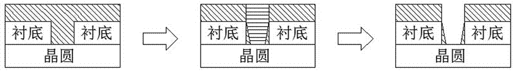
[0040] This embodiment continues to provide a deep trench photolithography process, using a negative resist to fill the deep trench, and the specific steps are as follows:

[0041] (1) Coat negative resist on the surface of the silicon dioxide substrate and in the deep groove. This negative resist is SG6200 negative resist produced by Fuji Film. This negative resist is insoluble in developer after exposure, but can be engraved eclipse;

[0042] (2) Expose the SG6200 negative glue in and above the deep groove, and remove the unexposed negative glue on the surface of the silicon dioxide substrate with a developer, so that the negative glue is filled in the deep groove;

[0043] (3) Coating a layer of American Rohm and Haas SEPR955 positive resist on the surface of the silica substrate and the surface of the organic material;

[0044] (4) Cover the SEPR955 positive resist above the silicon dioxide substrate with a mask plate to expose the SEPR955 positive resist above the deep g...


PUM


Abstract

The invention relates to an insulated gate bipolar transistor (IGBT) deep-trench photolithographic process, and belongs to the field of microelectronics. The IGBT deep-trench photolithographic process aims to solve the problem of insufficient photoetching of patterns at the bottom of a deep trench. The process comprises the following steps: (1), coating an organic material on the surface of a substrate and in the deep trench, wherein the organic material is insoluble in a developer and can be etched; (2), removing the organic material on the surface of the substrate to make the remaining organic material to be filled in the deep trench; (3), coating photoresist on the surface of the substrate and the surface of the organic material; (4), exposing the photoresist; (5), removing the photoresist on the deep trench by using the developer; (6), etching the organic material in the deep trench and a wafer at the bottom of the deep trench; and (7), removing the photoresist on the surface of the bottom of the substrate to complete the etching of the IGBT deep trench. The IGBT deep-trench photolithographic process has the advantages that the organic material is filled in the IGBT deep trench, so that sufficient and regular etching of the bottom of the deep trench can be realized.

Description

technical field [0001] The invention relates to an IGBT deep groove photolithography process, which belongs to the field of microelectronics. Background technique [0002] The photolithography process used in semiconductor technology is a multi-step pattern transfer process that is closer to photography. First, the required pattern is formed on the mask, and then the required pattern is transferred to each layer of the wafer surface through a photolithography process. [0003] The specific steps are as follows: 1. Coating, coating the surface of the wafer with a layer of photoresist. 2. Exposure, photoresist is a photosensitive substance, which is divided into two types, one is called positive resist, and the exposed part will change its own properties and structure, and will be soluble in developer. The other is called negative photoresist, which is the opposite of positive photoresist, and the unexposed part is soluble in developer solution. 3. Development, dissolve the...

Claims


Application Information

Patent Timeline
Patent Type & Authority Patents(China)
IPC IPC(8): H01L21/027H01L21/312H01L21/331G03F7/00
CPCH01L21/02112H01L21/0271H01L29/66325
Inventor 宋里千黄建伟罗海辉陈辉
Owner ZHUZHOU CRRC TIMES SEMICON CO LTD
Why Eureka
Try Eureka