A design method for improving etching yield of high-speed line pcb circuit board

A technology of PCB circuit board and design method, which is applied in the direction of removing conductive material by mechanical method, removing conductive material by chemical/electrolytic method, printing circuit, etc. In order to ensure the quality of finished products, improve the etching yield, and control the production cost

Active Publication Date: 2021-11-19
BRAIN POWER (QING YUAN) CO LTD
View PDF0 Cites 0 Cited by
  • Summary
  • Abstract
  • Description
  • Claims
  • Application Information

AI Technical Summary

Problems solved by technology

[0006] Aiming at the deficiencies of the prior art, the present invention provides a design method for improving the etching yield of high-speed line PCB circuit boards, which solves the problem that the existing method of removing copper foil is too single, and the etching method and the engraving method cannot be beneficially combined, resulting in etching The problem of low yield and high etching cost

Method used


Image

  • A design method for improving etching yield of high-speed line pcb circuit board
  • A design method for improving etching yield of high-speed line pcb circuit board

Examples


Embodiment

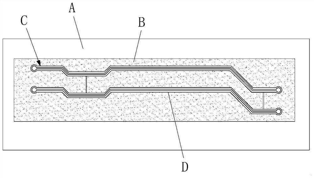
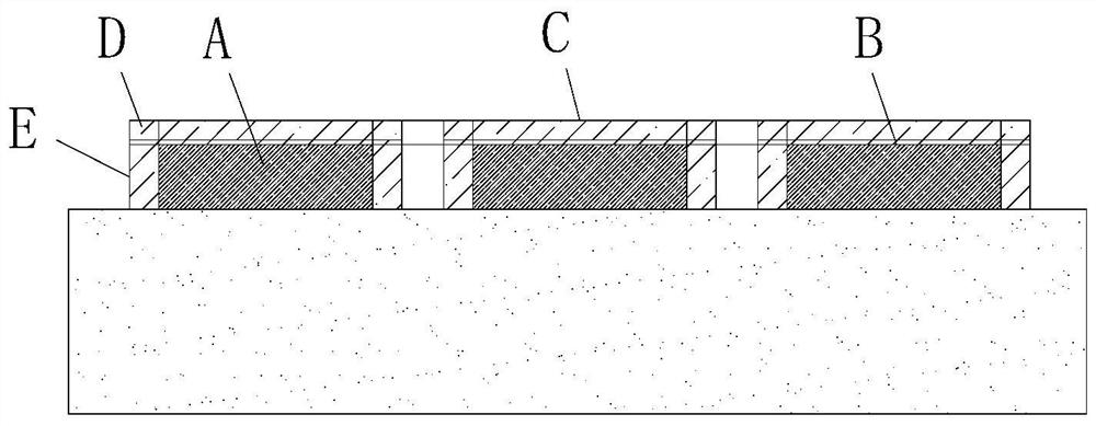
[0023] see Figure 1-2 , the present invention provides the following technical solutions: a high-speed line PCB circuit board design method for improving etching yield, comprising the following steps:

[0024] S1. Design A: Copper layer A is covered on the formed circuit board;

[0025] S2. Design B: pre-plating lead-tin resist layer B on copper layer A;

[0026] S3. Designs C and D: set up a printed etching board frame C that is suitable for the circuit wiring, and on the etching board frame C, there are edges D extending to both sides of the covered lead-tin resist layer B;

[0027] S4. Design E: remove the lead-tin resist layer B and the copper foil outside the edge D by chemical means, and form the side etching edge E corresponding to the upper and lower sides of the edge D on the copper layer A;

[0028] S5. Removal of E: use engraving method to mill out the side etching edge E.

[0029] Specifically, in S3, the manufacturing steps of the etching board frame C: carry ...


PUM


Abstract

The invention belongs to the technical field of PCB circuit board etching, in particular to a design method for improving the etching yield of a high-speed line PCB circuit board, comprising the following steps: S1, design A: covering a copper layer A on a formed circuit board; S2, design B: Pre-plate the lead-tin resist layer B on the copper layer A; S3, designs C and D: set the printed etching board frame C that is suitable for the circuit trace, and set the lead-tin covering on the etching board frame C The resist layer B extends along D on both sides. In the present invention, by arranging an etching plate frame and reserving edges extending to both sides of the covered lead-tin resist layer, it is possible to avoid the formation of "copper roots" on both sides of the lines, narrowing the line spacing, and at the same time avoiding a small part of the photosensitive film along the edges. Covering, leaving "residual glue" under the edge, the etching method and the engraving method are beneficially combined to achieve complete etching, which greatly improves the etching yield, effectively controls the production cost, and ensures the quality of the finished product.

Description

technical field [0001] The invention relates to the technical field of PCB circuit board etching, in particular to a design method for improving the etching yield of a high-speed line PCB circuit board. Background technique [0002] The process of the circuit board from the light board to the display of the circuit pattern is relatively complicated. At present, the typical process of circuit board (PCB) processing adopts the "pattern electroplating method", that is, first on the copper foil part that needs to be reserved on the outer layer of the circuit board, that is, the part of the circuit. A layer of lead-tin resist is pre-plated on the graphic part, and then the rest of the copper foil is chemically etched away, which is called etching. [0003] The existing copper removal methods generally adopt two methods: etching method and engraving method. The etching method is to use an etching solution to remove the copper foil other than the conductive circuit. The engraving m...

Claims


Application Information

Patent Timeline
Patent Type & Authority Patents(China)
IPC IPC(8): H05K3/06H05K3/04
CPCH05K3/04H05K3/061
Inventor 欧智鹏
Owner BRAIN POWER (QING YUAN) CO LTD
Why Eureka
Try Eureka