Array substrate, manufacturing method of array substrate and display device

A technology of array substrate and substrate substrate, which is applied in nonlinear optics, instruments, optics, etc., can solve problems such as the reduction of aperture ratio, achieve high aperture ratio, ensure display quality, and eliminate the effects of color resistance grooves

Active Publication Date: 2022-03-22
HKC CORP LTD
View PDF5 Cites 0 Cited by
  • Summary
  • Abstract
  • Description
  • Claims
  • Application Information

AI Technical Summary

Problems solved by technology

[0005] The purpose of the embodiment of the present application is to provide an array substrate, aiming to solve the problem of the common electrode between the color-resist layers of two adjacent sub-pixels in the existing display panel. The technical problem of reducing the aperture ratio caused by the need to widen the common electrode line due to overlapping above the line

Method used


Image

  • Array substrate, manufacturing method of array substrate and display device
  • Array substrate, manufacturing method of array substrate and display device
  • Array substrate, manufacturing method of array substrate and display device

Examples


Embodiment 1

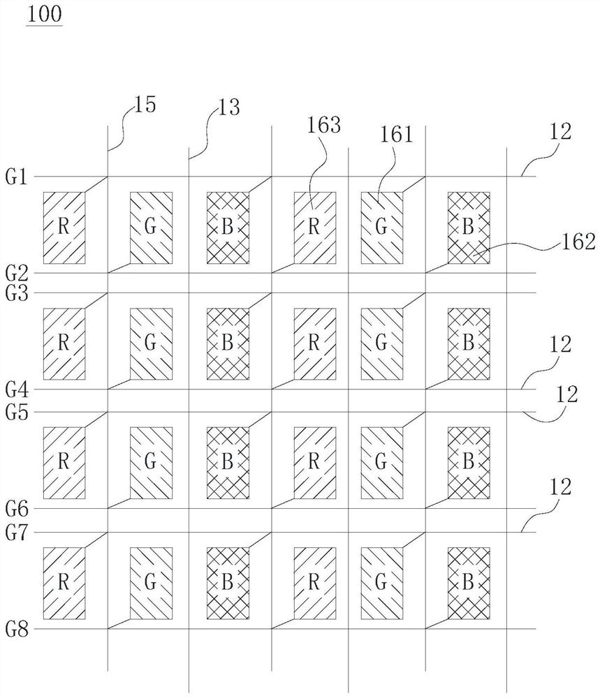
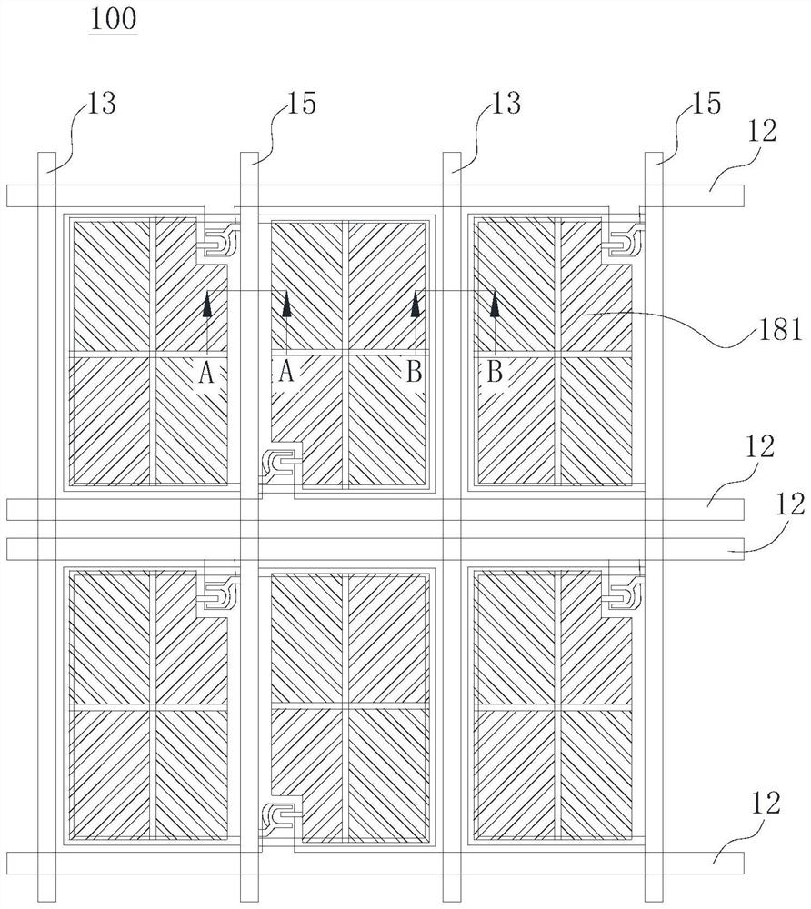
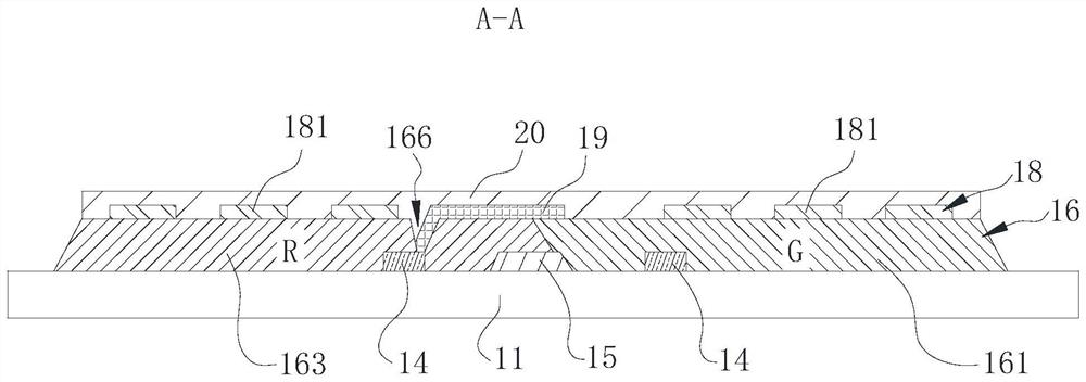
[0047] First, see figure 1 , image 3and Figure 4 As shown, Embodiment 1 of the present application provides an array substrate 100, which includes: a first base substrate 11, a common electrode line 13 and a data line 15 disposed on the first base substrate 11, and a common electrode line 13 disposed on the first base substrate 11. and the color resist layer 16 on the data line 15 , and the pixel electrode layer 18 disposed on the color resist layer 16 . Therefore, the array substrate 100 is a COT type array substrate.

[0048] Wherein, the color-resist layer 16 includes a plurality of color-resist blocks of different colors, namely a first color-resist block 161 , a second color-resist block 162 and a third color-resist block 163 . Such as figure 1 , figure 2 and Figure 4 As shown, the first color resistance block 161 and the second color resistance block 162 are adjacent in the direction perpendicular to the data line 15, and the edges of the two are located above ...

Embodiment 2

[0071] see Figure 5 As shown, compared with the first embodiment, the array substrate 100 provided by the second embodiment further includes a covering portion 172 disposed below the light shielding electrode 19 and above the color resist layer 16, that is, the covering portion 172 is formed on the first On the overlapping edges of the color-resist block 161 and the third color-resist block 163 , the light-shielding electrode 19 is further formed on the cover portion 172 .

[0072] The covering portion 172 is specifically strip-shaped and parallel to the data line 15 .

[0073]The purpose of this setting is that when the color-resist layer 16 is formed, it is necessary to deposit and etch color-resist material layers of different colors in multiple times, for example, first deposit and etch to form an R color-resist block, then deposit and etch to form a G color-resist block , and finally deposited and etched to form the B color-resist block, then, the edge of the first colo...

Embodiment 3

[0080] Figure 6 and Figure 7 Shown is the third embodiment of the array substrate 100 provided by the present application. The difference from the first and second embodiments above is that the flat layer 17 is generally a whole layer arranged between the pixel electrode layer 18 and the color resist layer 16 structure. Such as image 3 As shown, in addition to the filling portion 171 filling the color-resisting groove 160 and the covering portion 172 covering the overlapping edges of the first color-resisting block 161 and the third color-resisting block 163, the planar layer 17 also includes Each color resist block and the flat portion 173 above the filling portion 171 . Of course, it can be understood that the flat portion 173 needs to avoid the above-mentioned first via hole 166 and the second via hole.

[0081] That is to say, before forming the pixel electrode layer 18 and the light-shielding electrode 19, the color-resist trench 160 is filled with the flat layer 1...


PUM


Abstract

The invention is suitable for the technical field of display, and provides an array substrate, a manufacturing method and a display panel, the array substrate comprises a first substrate, a common electrode wire, a color resistance layer and a flat layer, the color resistance layer comprises a first color resistance block and a second color resistance block which are adjacent, according to the array substrate, the color resistance grooves located on the common electrode lines are formed between the first color resistance blocks and the second color resistance blocks, the first color resistance blocks and the second color resistance blocks are prevented from being overlapped above the common electrode lines, the width of the common electrode lines is small, and it can be guaranteed that the array substrate has the high aperture ratio; in addition, the array substrate further comprises a flat layer, and the color resistance grooves are filled with the filling parts of the flat layer. The color resistance grooves can be reduced or even eliminated, the adjacent first color resistance blocks and second color resistance blocks are flat, when a pixel electrode layer is formed on the color resistance layer in a deposition and etching mode, etching residues of transparent conductive materials in the color resistance grooves can be avoided, the etching yield is improved, and the display quality is guaranteed.

Description

technical field [0001] The present application relates to the field of display technology, and in particular to an array substrate, a manufacturing method of the array substrate, and a display device. Background technique [0002] The signal transmission of the liquid crystal display panel usually requires the use of Source COF (Source Chip On Film, source side chip on film) and Gate COF (Gate Chip On Film, gate side chip on film). With the gradual maturity of GOA (Gate Driveron Array, array substrate row drive technology) technology and its wider application range, Gate COF is no longer used, and the driving cost is mainly concentrated on Source COF, so reducing the number of Source COF can be effective Reduce the cost of LCD panels. When the resolution of the liquid crystal display panel is fixed, the number of source driving lines (that is, data lines) can be further reduced by changing the driving mode, so as to achieve the purpose of reducing the number of Source COFs....

Claims


Application Information

Patent Timeline
Patent Type & Authority Applications(China)
IPC IPC(8): G02F1/1362G02F1/1368G02F1/1333
CPCG02F1/136222G02F1/1368G02F1/133357G02F1/136286G02F1/1337G02F1/134309G02F1/13439G02F1/136209H01L27/1244H01L27/1248H01L27/1259
Inventor 黄世帅韩丙康报虹
Owner HKC CORP LTD
Why Eureka
Try Eureka