
Display panel and display device

A display panel and display area technology, which is applied in the direction of instruments, semiconductor devices, computing, etc., can solve the problems of too much etchant, the line width of the touch electrode becomes smaller, and breaks, and achieves the effect of improving the etching yield rate and the yield rate

Pending Publication Date: 2022-06-17
WUHAN CHINA STAR OPTOELECTRONICS SEMICON DISPLAY TECH CO LTD
View PDF0 Cites 0 Cited by
  • Summary
  • Abstract
  • Description
  • Claims
  • Application Information

AI Technical Summary

Problems solved by technology

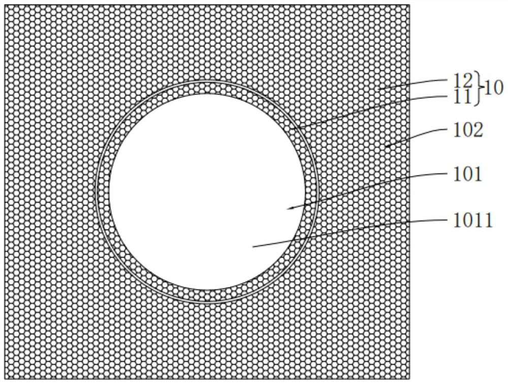
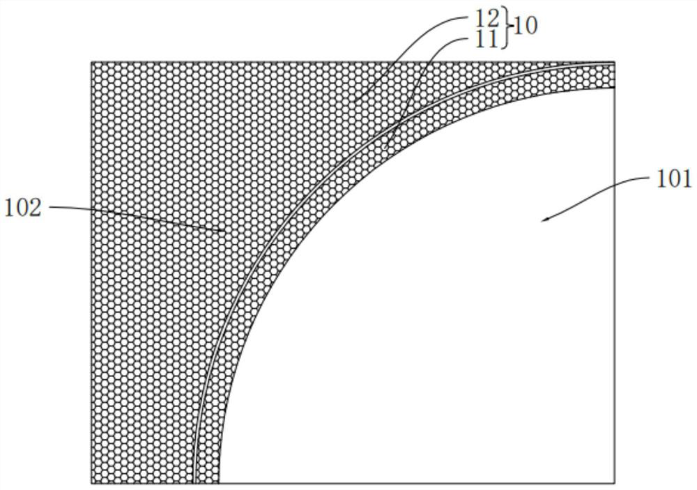
[0004] However, in the manufacturing process, etchant is usually used to pattern the touch layer metal to obtain touch electrode patterns and form openings in the CUP area. Since more touch layer metal is removed in the CUP area, the etchant required The amount of the touch electrode is more than that of other areas, which will cause the touch electrodes adjacent to the CUP area to be etched by the etchant in the CUP area during the etching process, which will easily make the line width of the touch electrodes adjacent to the CUP area smaller or even break and other adverse phenomena, thereby affecting the yield rate of OLED display panels

Method used


Image

  • Display panel and display device
  • Display panel and display device
  • Display panel and display device

Examples


Embodiment Construction

[0037] The technical solutions in the embodiments of the present invention will be clearly and completely described below with reference to the accompanying drawings in the embodiments of the present invention. Obviously, the described embodiments are only some, but not all, embodiments of the present invention. Based on the embodiments of the present invention, all other embodiments obtained by those skilled in the art without creative efforts shall fall within the protection scope of the present invention.

[0038] The following disclosure provides many different embodiments or examples for implementing different structures of the present invention. In order to simplify the disclosure of the present invention, the components and arrangements of specific examples are described below. Of course, they are only examples and are not intended to limit the invention. Furthermore, the present disclosure may repeat reference numerals and / or reference letters in different instances,...


PUM


Abstract

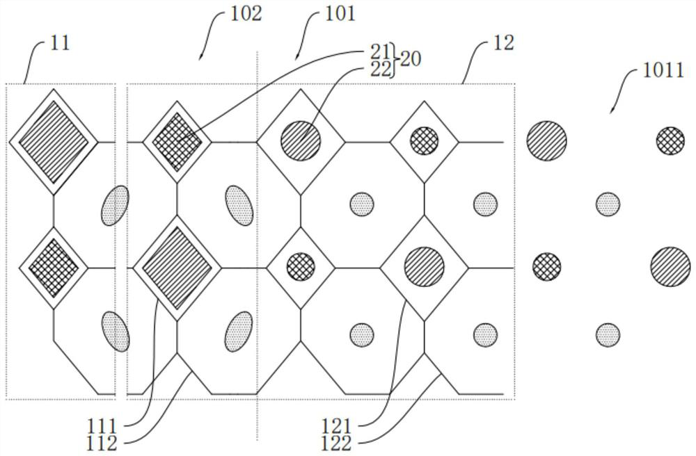
The invention discloses a display panel and a display device. The display panel comprises a function display area and a conventional display area; the display panel further comprises a substrate, a light-emitting layer and a touch layer. The light-emitting layer is arranged on the substrate and comprises a plurality of first light-emitting pixels arranged in the conventional display area and a plurality of second light-emitting pixels arranged in the functional display area, and in the same unit area, the number of the first light-emitting pixels is the same as that of the second light-emitting pixels; the touch control layer is arranged on the side, away from the substrate, of the light emitting layer and comprises an opening formed in the function display area, a blocking part arranged around the opening and a touch control part located on the side, away from the opening, of the blocking part, and the blocking part and the touch control part are arranged in an insulated mode; wherein at least part of the blocking part is arranged in the function display area, and the orthographic projection of the blocking part on the substrate is not overlapped with the orthographic projection of the first light-emitting pixels and the orthographic projection of the second light-emitting pixels on the substrate. According to the invention, the etching yield of the touch part and the yield of the display panel can be improved.

Description

technical field [0001] The present invention relates to the field of display technology, and in particular, to a display panel and a display device having the display panel. Background technique [0002] Organic light-emitting diode (Organic Light-Emitting Diode, OLED) display panels are widely used due to their advantages of self-luminescence, fast response speed, wide viewing angle, and flexible display. [0003] In order to increase the screen ratio of the display panel, the existing OLED display panel will be designed with an under-screen camera (CameraUnder Panel, CUP). In addition, in the related art, the touch layer is often arranged in the OLED display panel to improve the OLED display panel. increase the level of integration and reduce the thickness of the OLED display panel. In order to prevent the touch layer from affecting the light transmittance of the CUP area, the touch layer in the CUP area is often removed to improve the light transmittance of the CUP area,...

Claims


Application Information

Patent Timeline
Patent Type & Authority Applications(China)
IPC IPC(8): H01L27/32H01L21/77G06F3/041G06F3/044
CPCG06F3/0412G06F3/0446H10K59/40H10K59/12H10K59/1201G06F2203/04112H10K59/352H10K59/353H10K59/65
Inventor 王子怡
Owner WUHAN CHINA STAR OPTOELECTRONICS SEMICON DISPLAY TECH CO LTD
Learn More