SAB technique for semiconductor device

A process method and semiconductor technology, applied in semiconductor devices, electrical solid devices, electrical components, etc., can solve the problems of film filling holes, polysilicon gate pitch reduction, etc.

Active Publication Date: 2018-04-13
SHANGHAI HUALI MICROELECTRONICS CORP
View PDF4 Cites 0 Cited by
  • Summary
  • Abstract
  • Description
  • Claims
  • Application Information

AI Technical Summary

Problems solved by technology

The area reduction mainly starts with reducing the distance between the polysilicon gates of semiconductor devices, mainly MOS transistors. Usually, side walls need to be formed on the side of the polysilicon gate. Oxide layer sidewalls are formed. After the formation of double-layer sidewalls, the spacing between polysilicon gates will become smaller. Too small spacing between polysilicon gates will lead to voids (Void) in subsequent film filling.

Method used


Image

  • SAB technique for semiconductor device
  • SAB technique for semiconductor device
  • SAB technique for semiconductor device

Examples


Embodiment Construction

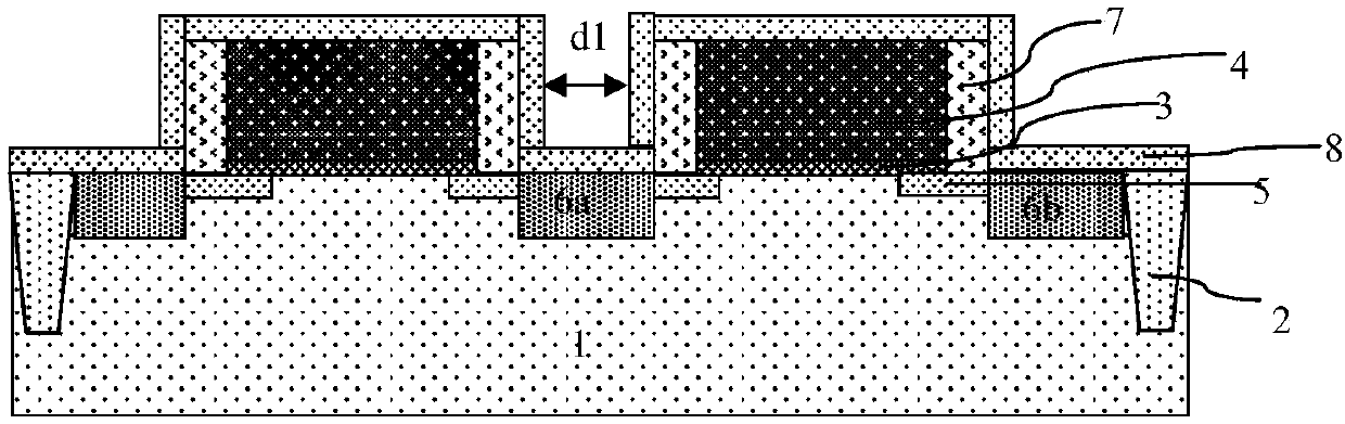
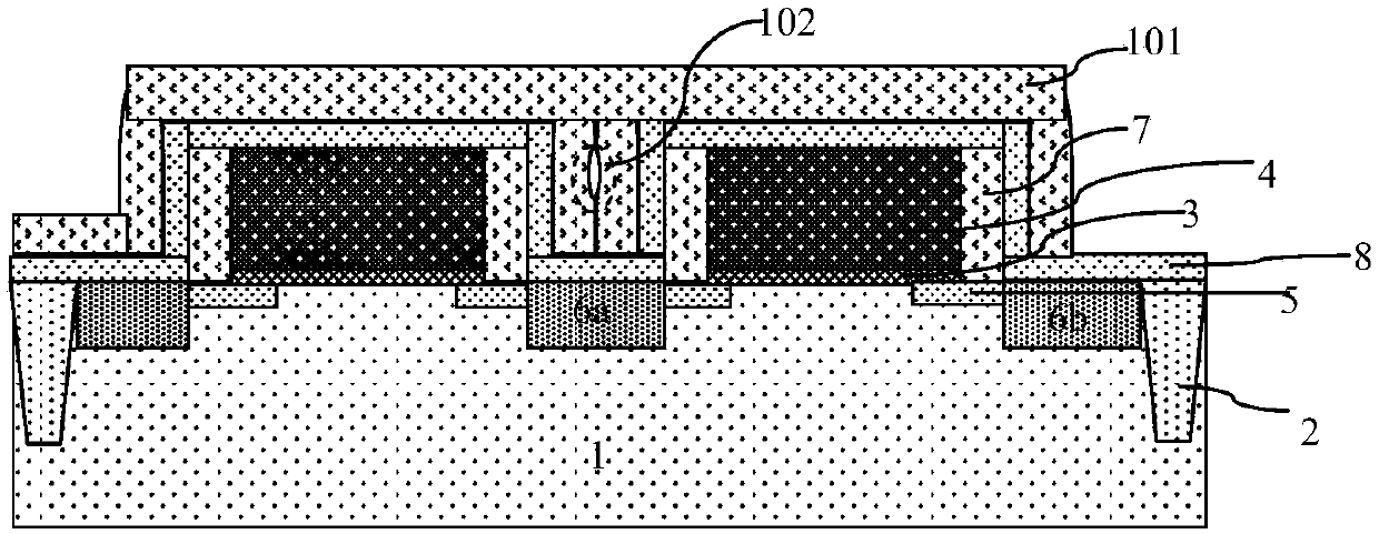
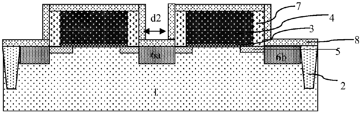
[0030] The existing method is obtained on the basis of analyzing the technical problems of the existing method, so before introducing the existing method in detail, describe the existing method; Figure 1A to Figure 1C As shown, it is a device structure diagram in each step of the SAB process method of the existing semiconductor device. The SAB process method of the existing semiconductor device includes the following steps:

[0031] Step 1, such as Figure 1A As shown, a gate structure, a source region 6a and a drain region 6b of a semiconductor device are formed, the gate structure includes a gate dielectric layer 3 and a polysilicon gate 4 sequentially formed on the surface of a semiconductor substrate 1, and the source region 6a and the drain region 6b are self-aligning quasi-formed on both sides of the corresponding polysilicon gate 4; the integration degree of the semiconductor device is improved by reducing the distance between two adjacent polysilicon gates 4. Figure...


PUM


Abstract

The invention discloses an SAB technique for a semiconductor device. The SAB technique comprises the steps of (1) forming a gate structure, source regions and drain regions of the semiconductor device; and (2) determining the required thickness of an SAB film and splitting a forming process of the SAB film by combining the spaces between polysilicon gates to ensure that no gap is formed between the polysilicon gates through the thickness of each SAB sub-film, photoetching the SAB sub-films, removing the SAB sub-film in an area in which metal silicide needs to be formed and achieving full etching of the SAB sub-film between the polysilicon gates, thereby preventing a void from appearing in the subsequent film forming process. According to the SAB technique, no void can be formed between thepolysilicon gates of the semiconductor layer in the process of forming the SAB film, so that the SAB film between the polysilicon gates can be fully etched and the SAB technique does not affect the spaces between the polysilicon gates, thereby facilitating filling of the film.

Description

technical field [0001] The invention relates to a method for manufacturing a semiconductor integrated circuit, in particular to a SAB process method for a semiconductor device. Background technique [0002] With the rapid development of mobile communications, display technology has also advanced rapidly. Due to the pursuit of higher resolution, larger capacity and larger size, higher requirements are placed on LCD display drivers. Among them, in order to meet the demand for larger capacity, it is necessary to continuously increase the capacity of the embedded SRAM on the basis of ensuring that the chip area remains unchanged, so it is necessary to continuously reduce the SRAM area, such as the SRAM area from 379μm 2 Shrink to 305μm 2 . The area reduction mainly starts with reducing the distance between the polysilicon gates of semiconductor devices, mainly MOS transistors. Usually, side walls need to be formed on the side of the polysilicon gate. Oxide layer sidewalls ar...

Claims


Application Information

Patent Timeline
Patent Type & Authority Applications(China)
IPC IPC(8): H01L27/11
CPCH10B10/00
Inventor 赵君红彭宇飞孙昌
Owner SHANGHAI HUALI MICROELECTRONICS CORP
Why Eureka
Try Eureka