Composite film and manufacturing method for manufacturing composite film
A production method and technology of composite film, applied in chemical instruments and methods, lamination auxiliary operations, synthetic resin layered products, etc., can solve problems such as affecting aesthetics and normal use, printing cursor and die-cutting position error, etc.
- Summary
- Abstract
- Description
- Claims
- Application Information
AI Technical Summary
Problems solved by technology
Method used
Image
Examples
Embodiment 2
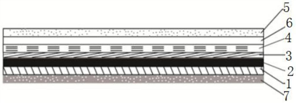
[0068] Such as Figure 4 Shown, on the other hand, the present invention provides a kind of manufacture method of making composite film again, wherein: comprise,
[0069] Step S110, providing a base film;
[0070] Step S120, performing composite glue treatment on the first predetermined layer of the base film;
[0071] Step S130, compounding the first predetermined layer of the base film and the second predetermined layer of the protective film and performing drying and curing treatment. After the drying treatment, the composite glue is cured, and the composite glue in the cured state completely composites the first predetermined layer of the base film and the second predetermined layer of the protective film.
[0072] As a further preferred embodiment, the above-mentioned method for making a composite film, wherein step S110, providing a base film specifically includes:
[0073] Step S11011, providing an initial film; wherein the initial film can be a PET / PVC film body, an...
specific Embodiment approach
[0097] Provide a PET base film with a thickness of 20-38um, corona treatment or chemical coating treatment on one side to increase its surface energy or polarity. The other side is coated with a matte coating, and the function of the matte coating is to prevent the film surface from being drawn during the production process.
[0098] Provide a PET protective film: thickness 15-35um, one side of the PET protective film is treated with corona, the other side is free of corona, and the information layer is coated on the corona surface. The information layer is generally acrylic resin or reactive polyurethane resin, and the thickness range : 1.0-2.0um; the optical micro-nano pattern (also can be understood as anti-counterfeiting pattern) is transferred to the film by molding, and a recognizable laser cursor is placed next to the pattern of each plate during molding; then the dielectric layer is evaporated to improve the optical micro-nano The reflectivity of the pattern. Coat the...
PUM
| Property | Measurement | Unit |
|---|---|---|
| Thickness | aaaaa | aaaaa |
| Thickness | aaaaa | aaaaa |
| Thickness | aaaaa | aaaaa |
Abstract
Description
Claims
Application Information


