Serdes architecture for 64B/66B conversion
A technology of a transmitting device and a receiving device, applied in the field of serdes architecture, can solve the problem of high chip design complexity, and achieve the effects of reducing operating frequency and logic complexity, reducing timing requirements, and reducing chip design costs
- Summary
- Abstract
- Description
- Claims
- Application Information
AI Technical Summary
Problems solved by technology
Method used
Image
Examples
Embodiment Construction
[0023] The present invention will be further described below in conjunction with the accompanying drawings and embodiments.
[0024] It should be noted that all directional indications (such as up, down, left, right, front, back, inside, outside, top, bottom...) in the embodiments of the present invention are only used to explain As shown in the figure), if the relative positional relationship between the various components, etc., if the specific posture changes, the directional indication will also change accordingly.
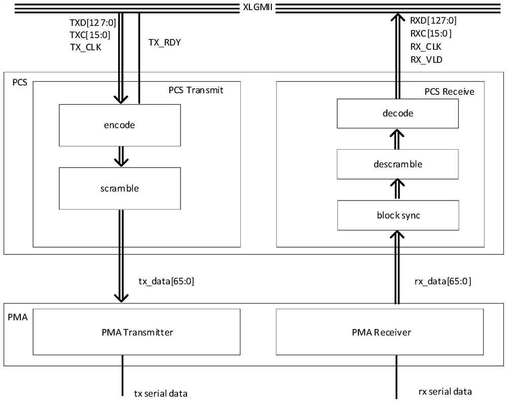
[0025] The embodiment of the present invention provides a serdes architecture for 64B / 66B conversion, including XLGMII (Media Independent Interface, Media Independent Interface), a PCS layer and a PMA layer, and the interface bit width of the PCS layer and the PMA layer is configured to be 66 bits.
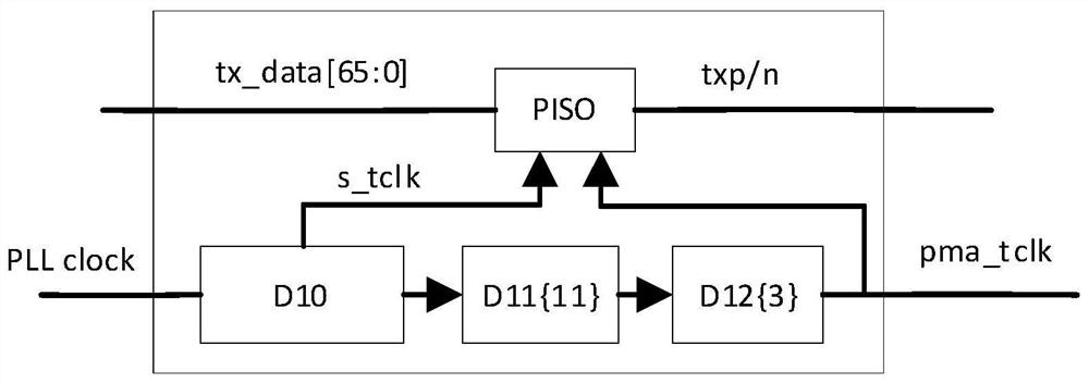
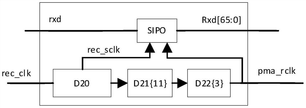
[0026] The 64B / 66B converted serdes architecture of the present invention reduces the number of internal clocks in the PCS by configuring the PCS and the interfac...
PUM
 Abstract
Description
Claims
Application Information


