Test development method and device for selection through AD conversion result

A technology to be tested and a testing machine, applied in the direction of measuring devices, electronic circuit testing, automated testing systems, etc., can solve the problems of increasing chip design area, increasing chip manufacturing cost, occupying chips, etc., to facilitate development and debugging, and reduce quantity requirements, the effect of cost reduction

Active Publication Date: 2021-03-26
苏州英嘉通半导体有限公司
View PDF13 Cites 0 Cited by
  • Summary
  • Abstract
  • Description
  • Claims
  • Application Information

AI Technical Summary

Problems solved by technology

[0003]At present, in order to cope with the mass production test of chips, it is more popular in chip design to design chip test mode and insert DFT (Design For Test) design. This method can greatly simplify the mass production test development, but the additional design circuit will greatly increase the design area of ​​the chip and increase the manufacturing cost of the chip. At the same time, these two test methods need to occupy a certain number of test pins on the chip. Chips with low cost and few pins are not applicable

Method used


Image

  • Test development method and device for selection through AD conversion result
  • Test development method and device for selection through AD conversion result
  • Test development method and device for selection through AD conversion result

Examples


Embodiment 1

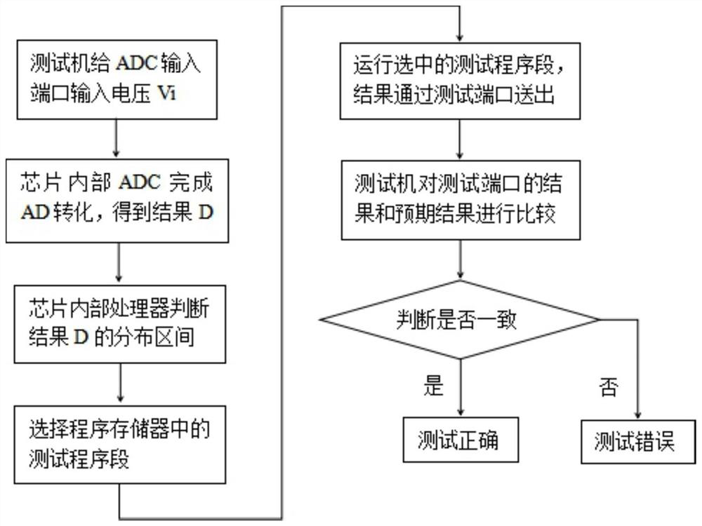
[0029] Assuming that the internal ADC module of the chip to be tested is a 12-bit successive approximation type AD, and the AD precision is 8 bits, the minimum conversion result of the AD conversion is 0, and the maximum conversion result is 2 12 -1=4095, the error range of the conversion result is -2 4 ~2 4 , that is -16~16, the number of test items distinguished by the conversion result of AD is at least 2 7 =128; Assume that the positive reference voltage of the internal AD is 3V, and the negative reference voltage is 0V, then the voltage range input by the AD input port is 0V ~ 3V, and the minimum interval of the input voltage of the test item selected by the input voltage is 24mV ( 3000 / 128≈24).

[0030] Assuming that the test items to be completed by the chip to be tested are 30 items, the numbers of the test items are respectively Ti (i=1~30), and the input voltage intervals corresponding to different test items are 100mV, then the test is carried out as follows:

[...


PUM


Abstract

The invention discloses a test development method and device for selection through an AD conversion result, and the device comprises a test machine for testing a to-be-tested chip, the test machine comprises a voltage supply unit for supplying power to the to-be-tested chip, a measurement unit, and a data processing unit, and the test unit is connected with the data processing unit. The voltage supply unit is connected with an ADC input port of a to-be-tested chip, and the test unit is connected with a test port of the to-be-tested chip. According to the invention, the characteristic that mostdigital, analog or digital-analog hybrid chips on the market at present are provided with internal ADC modules and storage units is effectively utilized, the development convenience of mass production test is improved, and the mass production test cost is reduced.

Description

technical field [0001] The invention relates to a test development method and device for selection through AD conversion results, and belongs to the technical field of chip mass production testing. Background technique [0002] As the scale of chip integrated circuits continues to increase, more and more functions and parameters need to be tested. How to reduce the time and difficulty of mass production test development as much as possible while ensuring mass production test coverage, become very important. [0003] At present, in order to cope with the mass production test of the chip, it is more popular in the chip design to design the test mode of the chip and insert the DFT (Design For Test) design. These two methods can indeed greatly simplify the mass production test development, but the additional Designing the circuit will greatly increase the design area of ​​the chip and increase the manufacturing cost of the chip. At the same time, both of these two test methods ...

Claims


Application Information

Patent Timeline
Patent Type & Authority Applications(China)
IPC IPC(8): G01R31/28
CPCG01R31/2851G01R31/2834
Inventor 陈丽萍陈辉柳永胜胡峰白强唐瑜吴文英于洁
Owner 苏州英嘉通半导体有限公司
Why Eureka
Try Eureka