
Overturning positioning structure for semiconductor insulating sheath pressing device

A technology of insulating sheath and pressing device, which is applied in semiconductor/solid-state device manufacturing, electrical components, circuits, etc. It can solve the problems of inconvenient pressing block positioning, single use mode, and inconvenient turning device, so as to shorten the molding time and design Reasonable and easy to operate

Inactive Publication Date: 2021-03-30
江西超弦光电科技有限公司
View PDF19 Cites 0 Cited by
  • Summary
  • Abstract
  • Description
  • Claims
  • Application Information

AI Technical Summary

Problems solved by technology

[0005] The purpose of the present invention is to provide a flipping positioning structure for a semiconductor insulating sheath pressing device, which aims to improve the flipping device for a semiconductor insulating sheath pressing device in the prior art. Due to its own design characteristics, the structure is simple and the way of use Single, in the actual use process, it is not convenient to locate the turning device, so it is not convenient to locate the pressing block in the pressing process, and in the actual use process, it is not convenient to guide the moving direction of the turning device, It is easy to cause the pressing block to shift in the horizontal direction of movement, thereby reducing the quality of the pressing and forming of the insulating sheath

Method used


Image

  • Overturning positioning structure for semiconductor insulating sheath pressing device
  • Overturning positioning structure for semiconductor insulating sheath pressing device
  • Overturning positioning structure for semiconductor insulating sheath pressing device

Examples


Embodiment Construction

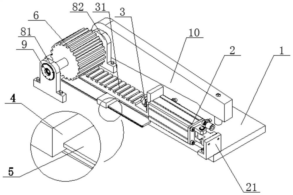
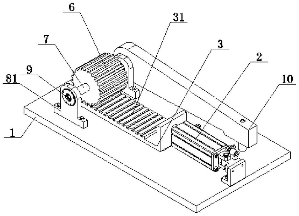
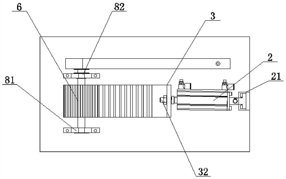
[0023] Please refer to figure 1 , figure 2 , image 3 , Figure 4 , Figure 5 with Figure 6 According to the present invention, it provides a technical solution: a flip position structure of a semiconductor insulating sheathed press, including a fixed base 1, a hydraulic cylinder 2 disposed at one end of the fixed base 1 for fixing the hydraulic cylinder 2 The connecting shaft 33 connected to the telescopic axis of the hydraulic cylinder 2 is disposed at the movable plate 3 connected to the connecting shaft 33, and the sliding seat 4 at the lower end of the moving plate 3 is disposed, and the slide rail 5 in cooperation with the sliding seat 4, uniform The rack 31 provided on the end surface of the moving board 3, the gear 6, which is engaged with the rack 31, the rotating shaft 7 connected to the gear 6, for the first support seat 81 and the second support 82 for supporting the rotary shaft 7. The block 10 connected to one end of the rotating shaft 7 is disposed on the press ho...


PUM


Abstract

An overturning positioning structure for a semiconductor insulating sheath pressing device comprises a fixed base, a hydraulic air cylinder, a fixed base, a connecting shaft, a movable plate, a sliding base, a sliding rail, a rack, a gear, a rotating shaft, a first supporting base, a second supporting base, a pressing block, a pressing hole, a forming column head, a supporting column and a heatingrod body. According to the overturning positioning structure for the semiconductor insulating sheath pressing device, the moving plate is driven to rotate through the telescopic shaft of the hydraulic cylinder, and the rack on the upper end surface of the moving plate is engaged with the gear, so that the telescopic motion of the hydraulic cylinder is conveniently converted into rotary motion, and the rotating shaft is conveniently driven to rotate through the gear; and therefore, the rotating shaft can conveniently drive the pressing block to rotate, the rotating angle of the pressing blockcan be conveniently limited through the meshing effect of the racks, and the rotated pressing block can be conveniently positioned.

Description

Technical field [0001] The present invention relates to the technical field of semiconductor processing apparatus, and in particular, a semiconductor insulating sheathed pressed device flip position structure. Background technique [0002] The semiconductor is a substance between the conductivity between the insulator to the conductor. The electrical conductivity is easily controlled, and can be used as an element material for information processing; from the perspective of technology or economic development, the semiconductor is very important; many electronic products, such as Computer, mobile phones, and digital recorders are used to process information using the electrical conductivity of semiconductors; common semiconductor materials silicon, germanium, gallium gallium gallium, and silicon are more in various semiconductor materials; [0003] The flip device in the prior art is in the actual use of the semiconductor insulation sheathed press, which is simple to use, and is n...

Claims


Application Information

Patent Timeline
Patent Type & Authority Applications(China)
IPC IPC(8): H01L21/67
CPCH01L21/67092H01L21/67121H01L21/67011
Inventor 郑德仁
Owner 江西超弦光电科技有限公司
Learn More