Three-dimensional memory structure and preparation method thereof

A memory, three-dimensional technology, applied in the direction of electric solid devices, semiconductor devices, electrical components, etc., can solve the problems of contact, affecting the reliability of the device, and the problem of step support in the step area, and achieve the effect of strengthening the structure and improving the collapse phenomenon.

Pending Publication Date: 2021-04-06
YANGTZE MEMORY TECH CO LTD
View PDF18 Cites 1 Cited by
  • Summary
  • Abstract
  • Description
  • Claims
  • Application Information

AI Technical Summary

Problems solved by technology

In this process, since the dummy channel hole in the step region is filled with silicon oxide, when the ONO structure at the bottom of the vertical channel structure in the core region is removed, the silicon oxide in the dummy channel hole in the step region will also were removed together, causing problems with step supports in the step area
[0003] In addition, in the three-dimensional memory based on back selection, metal contacts and peripheral conductive pillars connected to metal contacts are prone to direct contact with highly doped polysilicon at the bottom, which will affect the reliability of the device

Method used


Image

  • Three-dimensional memory structure and preparation method thereof
  • Three-dimensional memory structure and preparation method thereof
  • Three-dimensional memory structure and preparation method thereof

Examples


Embodiment 1

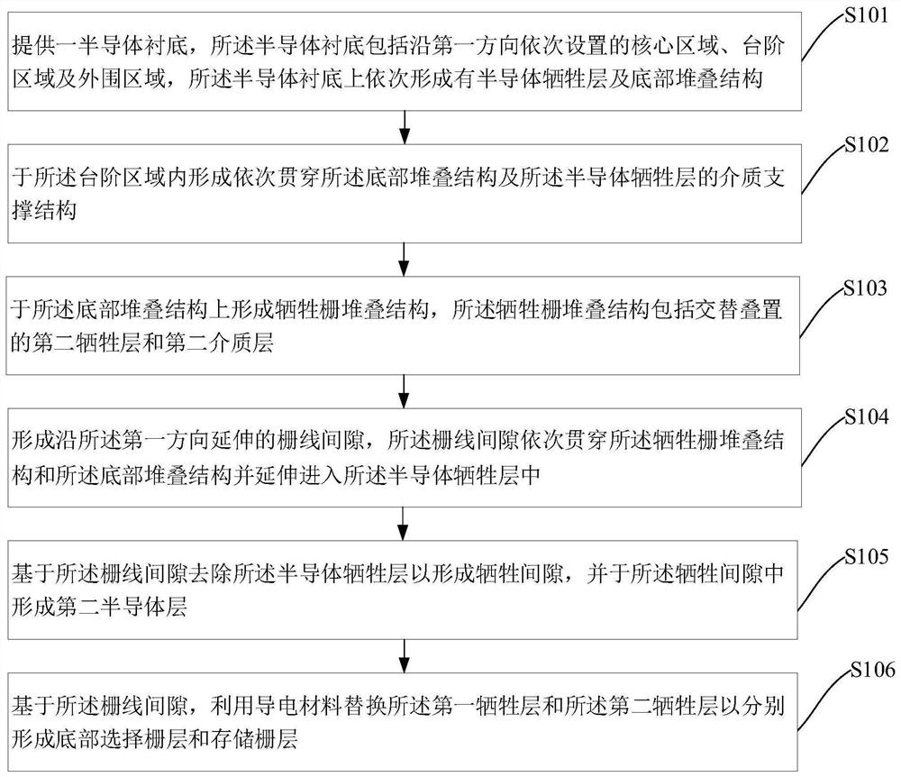
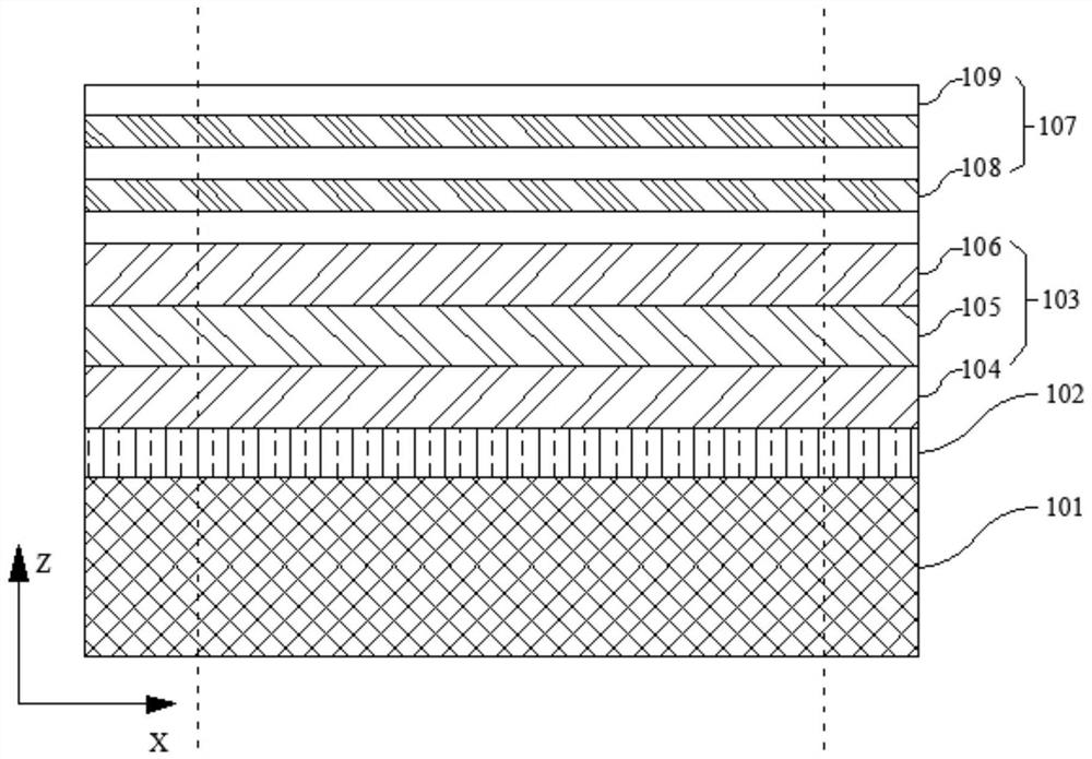
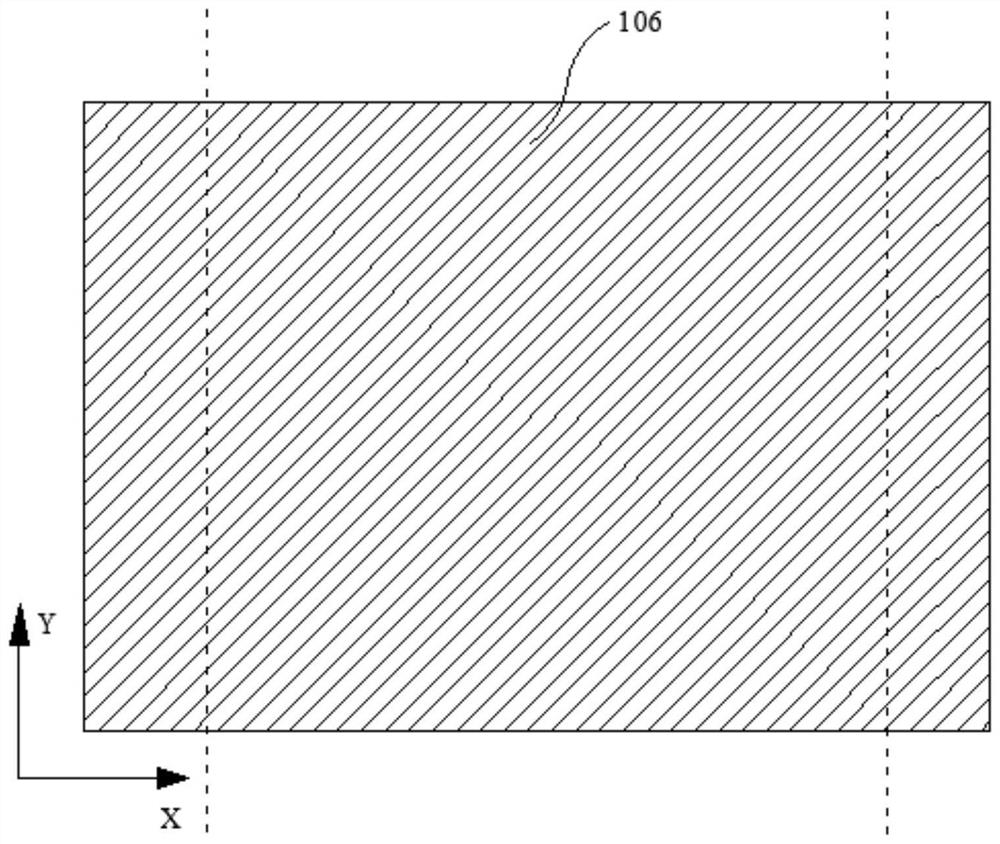
[0115] This embodiment introduces a method for preparing a three-dimensional memory structure, wherein, figure 1 A schematic flow chart showing a method for preparing a three-dimensional memory structure in this embodiment, figure 2 , 4 , 6 and 8 respectively show the cross-sectional schematic diagrams corresponding to different process steps in the preparation process of the three-dimensional memory structure, image 3 , 5 , 7 and 9 show the corresponding figure 2 , 4 The top view along the top surface of the third semiconductor layer 106 in the devices in the structures of , 6 and 8 .

[0116] The method for preparing the three-dimensional memory structure of this embodiment will be described in detail below in conjunction with the schematic diagrams corresponding to each step.

[0117] First, see Figure 1-3 , execute step S101: provide a semiconductor substrate 101, the semiconductor substrate 101 includes a core area, a step area and a peripheral area (correspondi...

Embodiment 2

[0134] This embodiment introduces another method for preparing a three-dimensional memory structure, wherein, figure 1 A schematic flow chart showing a method for preparing a three-dimensional memory structure in this embodiment, Figure 10 , 12 , 14 and 16 respectively show cross-sectional schematic diagrams corresponding to different process steps in the preparation process of the three-dimensional memory structure, Figure 11 , 13 , 15 and 17 respectively show the corresponding Figure 10 , 12 , 14 and 16 are top views along the top surface of the third semiconductor layer 106 .

[0135] The difference between this embodiment and Embodiment 1 is that the shape of the dielectric support structure 111 in step S102 is different. In this embodiment, the dielectric support structure 111 is an annular dielectric support structure, while in the first embodiment It is a solid dielectric support structure 111, and other structures are basically the same, so they will not be des...

Embodiment 3

[0139] This embodiment introduces the preparation method of the third three-dimensional memory structure. The difference between this embodiment and the first embodiment lies in that the shape of the peripheral filling structure 113 in step S102 is different, and other structures are basically the same, so details are not repeated here.

[0140] Specifically, see Figure 18 , in this embodiment, the peripheral groove is an annular groove, the peripheral filling structure 113 formed in the peripheral groove is an annular peripheral filling structure, and the annular peripheral filling structure is a rectangular annular structure , of course it can also be a circular ring, an elliptical ring or other closed ring structures. Since the first semiconductor layer 104 , the semiconductor sacrificial layer 105 , and the third semiconductor layer 106 inside the annular peripheral groove are retained during etching of the peripheral groove, this can effectively reduce the internal stre...


PUM


Abstract

The invention provides a three-dimensional memory structure and a preparation method thereof. The three-dimensional memory structure comprises a semiconductor layer, a bottom selection gate stack structure, a dielectric supporting structure, a storage gate stacking structure and a grid line gap, wherein thesemiconductor layer comprises a core region, a step region and a peripheral region which are sequentially arranged along a first direction; the bottom selection gate stack structure is formed on the semiconductor layer; the dielectric supporting structure is located in the step region, and the dielectric supporting structure sequentially penetrates through the bottom selection gate stack structure and the semiconductor layer; the storage gate stacking structure is formed on the bottom selection gate stack structure; and the grid line gap extends along the first direction, and the grid line gap sequentially penetrates through the storage grid stack structure and the bottom selection grid stack structure and extends into the semiconductor layer. By utilizing the structure, the dielectric supporting structure is not damaged when the semiconductor sacrificial layer is removed based on grid line gap etching, the dielectric supporting structure plays a supporting role, and the collapse phenomenon in the etching process of the three-dimensional memory structure is improved.

Description

technical field [0001] The invention belongs to the field of semiconductor design and manufacture, and in particular relates to a three-dimensional memory structure and a preparation method thereof. Background technique [0002] The semiconductor substrate of the three-dimensional memory has a stacked structure, and the vertical channel structure is located in the stacked structure and runs through the stacked structure. When the stacked structure (including stacked silicon nitride and oxide films) is deposited on the semiconductor substrate, the semiconductor A sacrificial polysilicon layer is introduced between the substrate and the stacked structure. After the gate line gap is etched, it is necessary to deposit various protective films in the gate line gap and perform multiple etchings. Then, based on the gate line gap, the sacrificial polysilicon layer and the The functional sidewall of the vertical channel structure surrounding the position of the sacrificial polysilico...

Claims


Application Information

Patent Timeline
Patent Type & Authority Applications(China)
IPC IPC(8): H01L27/11565H01L27/1157H01L27/11573H01L27/11582
CPCH10B43/10H10B43/40H10B43/35H10B43/27
Inventor 孔翠翠张坤吴林春张中周文犀
Owner YANGTZE MEMORY TECH CO LTD
Why Eureka
Try Eureka