Gallium nitride power device structure and preparation method
A power device, gallium nitride technology, applied in semiconductor/solid-state device manufacturing, electric solid-state devices, semiconductor devices, etc., can solve problems affecting device power density and power added efficiency performance, current collapse, etc.
- Summary
- Abstract
- Description
- Claims
- Application Information
AI Technical Summary
Problems solved by technology
Method used
Image
Examples
Embodiment 1
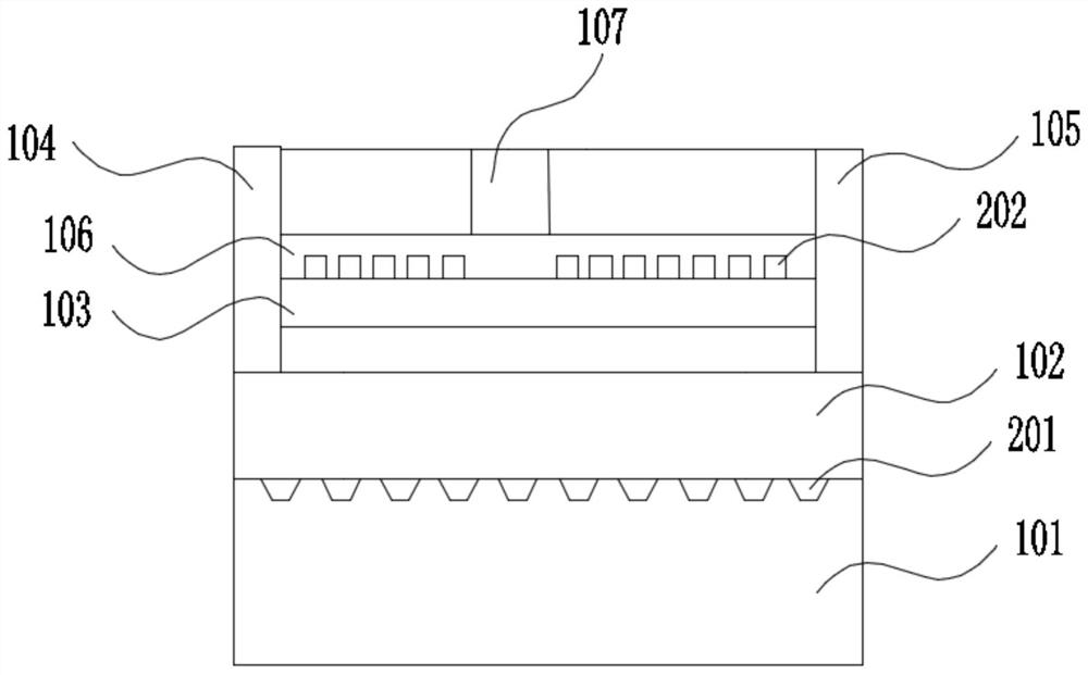
[0034] A gallium nitride power device structure, comprising a substrate 101, an AlGaN barrier layer 103, and a gate dielectric layer 106, the upper surface of the substrate 101 is provided with a first microwell structure 201, and the first microwell structure 201 is parallel to Multiple groups are set; the upper surface of the AlGaN barrier layer 103 is provided with a second microwell structure 202, and multiple groups of the second microwell structure 202 are arranged in parallel, and the gate dielectric layer 106 is grown on the AlGaN barrier layer 103 , multiple groups of grooves are arranged parallel to the lower surface of the gate dielectric layer 106 and embedded with the second microwell structure 202 on the upper surface of the AlGaN barrier layer 103 .
Embodiment 2
[0036] This embodiment is further improved based on Embodiment 1, the substrate 101 is a Si substrate, the upper surface of the Si substrate 101 is etched to form the first microwell structure 201, and the first microwell structure 201 The cross section is an inverted trapezoid, and the angle of the hypotenuse of the inverted trapezoid is 54°; the etching solution for etching the upper surface of the Si substrate 101 is NaOH or KOH etching solution. ; Also includes a gate 107, the gate 107 is located on the gate dielectric layer 106, the contact type between the gate 107 and the gate dielectric layer 106 is set as a Schottky contact; also includes a source 104, Drain 105, GaN buffer layer 102, the GaN buffer layer 102 is located on the substrate 101, the source 104 and the drain 105 are located on the GaN buffer layer 102 and the AlGaN barrier layer 103 and gate The dielectric layer 106 is located between the source electrode 104 and the drain electrode 105, and the contact ty...
Embodiment 3
[0046] The difference between this embodiment and Embodiment 2 is that the substrate is a non-Si substrate 101, and this embodiment uses a GaN substrate, and the upper surface of the substrate 101 is etched to form the first microwell structure 201, The cross section of the first microwell structure 201 is rectangular.
[0047] In this embodiment, a GaN substrate is used to etch and form multiple sets of parallel rectangular micro-well structures on the substrate surface, so that the heat dissipation area of the interface between the GaN buffer layer and the substrate can be increased to achieve a good heat dissipation effect.
PUM
 Abstract
Description
Claims
Application Information
 - R&D
- Intellectual Property
- Life Sciences
- Materials
- Tech Scout
- Unparalleled Data Quality
- Higher Quality Content
- 60% Fewer Hallucinations
Browse by: Latest US Patents, China's latest patents, Technical Efficacy Thesaurus, Application Domain, Technology Topic, Popular Technical Reports.
© 2025 PatSnap. All rights reserved.Legal|Privacy policy|Modern Slavery Act Transparency Statement|Sitemap|About US| Contact US: help@patsnap.com

