Display panel and preparation method thereof, and display device

A technology for a display panel and a manufacturing method, which is applied in the fields of display devices, display panels and their preparation, and display device manufacturing, and can solve problems such as cracks, encapsulation layer punctures, and inability to ensure zero pollution in the cavity

Active Publication Date: 2021-04-06
WUHAN CHINA STAR OPTOELECTRONICS SEMICON DISPLAY TECH CO LTD
View PDF16 Cites 0 Cited by
  • Summary
  • Abstract
  • Description
  • Claims
  • Application Information

AI Technical Summary

Problems solved by technology

However, zero pollution in the cavity cannot be guaranteed when using evaporation technology to manufacture OLED devices. Foreign particles will exist on the surface of the formed OLED device, and the packaging layer formed on the OLED device for encapsulating the OLED device is relatively thin,

Method used


Image

  • Display panel and preparation method thereof, and display device
  • Display panel and preparation method thereof, and display device
  • Display panel and preparation method thereof, and display device

Examples


Embodiment Construction

[0041] The technical solutions in the embodiments of the present invention will be clearly and completely described below in conjunction with the drawings in the embodiments of the present invention. Apparently, the described embodiments are only some of the embodiments of the present invention, but not all of them. Based on the embodiments of the present invention, all other embodiments obtained by those skilled in the art without creative efforts fall within the protection scope of the present invention.

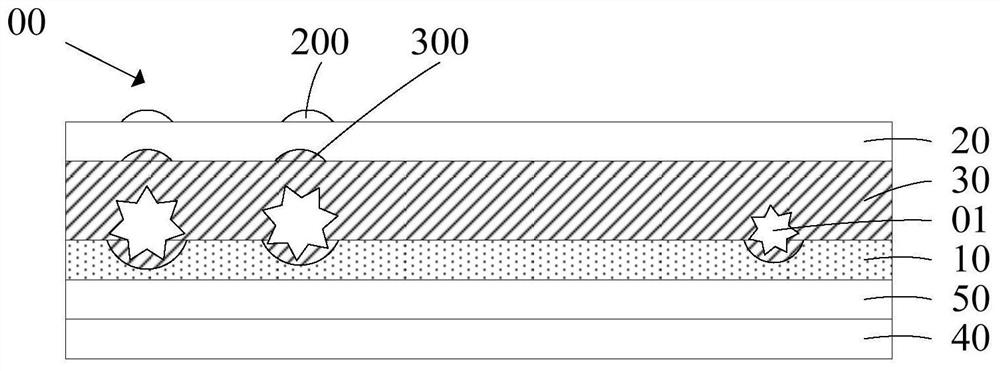
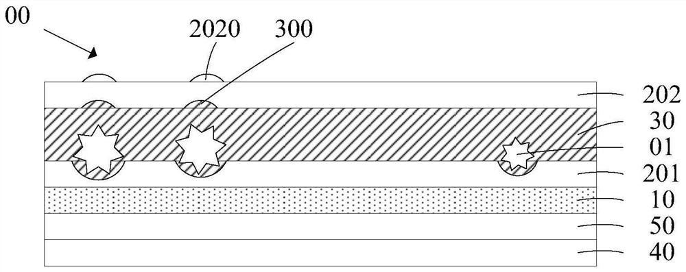
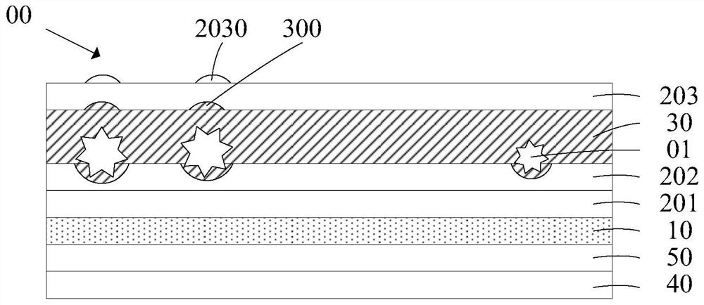
[0042] In the description of the present invention, it should be understood that the orientation or positional relationship indicated by the terms "upper", "lower", "away" and the like are based on the orientation or positional relationship shown in the drawings, for example, "upper" is just a superficial Above the object, it can specifically refer to directly above, obliquely above, or the upper surface, as long as it is above the level of the object; the above orientatio...


PUM


Abstract

The invention provides a display panel and a manufacturing method thereof, and a display device. The display panel comprises a light-emitting layer, a packaging layer, a correction layer and a plurality of particles, wherein the packaging layer is located on the light-emitting layer; and when the plurality of particles are located between the light-emitting layer and the packaging layer, the correction layer is located on the light-emitting layer and the plurality of particles, and the correction layer wraps the plurality of particles. According to the above scheme, the plurality of the particles can be wrapped by the correction layer, so the risk that the packaging layer is punctured by the plurality of the particles or cracks occur is reduced, and the reliability of thin film packaging is improved so as to reduce the risk that an OLED device is damaged.

Description

technical field [0001] The present invention relates to the field of display technology, in particular to the manufacture of display devices, in particular to a display panel, a preparation method thereof, and a display device. Background technique [0002] The OLED (Organic Light Emitting Diode, Organic Light Emitting Diode) display panel adopts self-luminous technology for image display, and has the advantages of fast response speed, high contrast ratio, and wide viewing angle. [0003] Among them, the biggest advantage of OLED lies in the production of flexible panels, and OLED packaging technology is mainly thin film packaging. However, zero pollution in the cavity cannot be guaranteed when using evaporation technology to manufacture OLED devices. Foreign particles will exist on the surface of the formed OLED device, and the packaging layer formed on the OLED device for encapsulating the OLED device is relatively thin, resulting in It is very easy to be punctured or cra...

Claims


Application Information

Patent Timeline
IPC IPC(8): H01L51/52H01L51/56H01L27/32
CPCH10K59/40H10K59/12H10K50/844H10K71/00
Inventor 赵宸
Owner WUHAN CHINA STAR OPTOELECTRONICS SEMICON DISPLAY TECH CO LTD
Why Eureka
Try Eureka