
Semiconductor glaze layer sintering method for improving matching degree of semiconductor part and central electrode
A technology of center electrode and sintering method, which is applied to spark gap parts, circuits, electrical components, etc., can solve the problems of loose fit between semiconductor components and center electrodes, increased insulation resistance, uneven glaze layer, etc., to avoid the fit The effect of poor temperature, improved ignition performance, and little difficulty in operation
- Summary
- Abstract
- Description
- Claims
- Application Information
AI Technical Summary
Problems solved by technology
Method used
Image

Examples
Embodiment 1
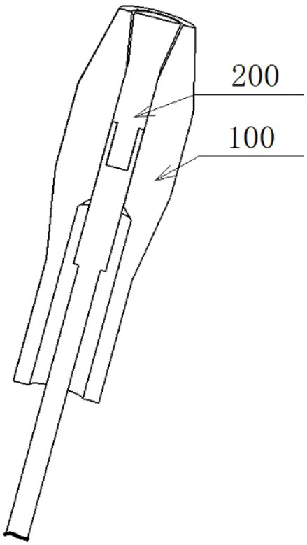
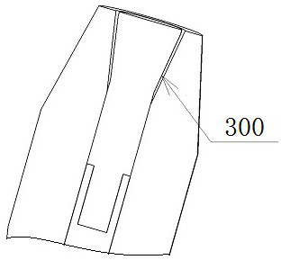
[0024] The semiconductor glaze layer 300 sintering method for improving the matching degree of the semiconductor component and the central electrode is to firstly make the central electrode wax mold 200 according to the shape and size of the central electrode, then fit the porcelain tube 100 with the central electrode wax mold 200, and connect the outer cone surface of the central electrode with the central electrode wax mold 200. The pre-configured semiconductor enamel is injected into the interstices of the inner conical surfaces of the porcelain tube 100. After the semiconductor enamel cools naturally, it is placed on the high-alumina tiles, and the high-alumina tiles placed on the porcelain tube 100 are placed on the high-alumina tiles at a rate of one piece every 15 minutes. The aluminum tiles are sent into a high temperature furnace for sintering.
[0025] Among them, 38-40 parts of potassium feldspar, 42-44 parts of quartz, 7-8 parts of kaolin, 3-4 parts of magnesium car...
PUM
 Abstract
Description
Claims
Application Information