Coated wafer correction equipment

A technology for calibrating equipment and wafers, applied in sputtering coating, ion implantation coating, vacuum evaporation coating and other directions, which can solve the problems of different coating areas, affecting subsequent use, etc., to improve stability and speed of correction Effect

Pending Publication Date: 2021-04-09
HEFEI JINGWEITE ELECTRONICS CO LTD
View PDF0 Cites 0 Cited by
  • Summary
  • Abstract
  • Description
  • Claims
  • Application Information

AI Technical Summary

Problems solved by technology

[0003] When coating piezoelectric wafers, the piezoelectric wafers are placed on the calibration plate by an automated robotic arm. Due to the slight distance error during placement, the distances between all piezoelectric wafers may be different, resulting in subsequent sputtering coatings. , the coating area on each piezoelectric chip is different, which will affect the subsequent use, so it needs to be solved urgently

Method used


Image

  • Coated wafer correction equipment
  • Coated wafer correction equipment
  • Coated wafer correction equipment

Examples


Embodiment Construction

[0027] The following will clearly and completely describe the technical solutions in the embodiments of the present invention with reference to the accompanying drawings in the embodiments of the present invention. Obviously, the described embodiments are only some, not all, embodiments of the present invention. Based on the embodiments of the present invention, all other embodiments obtained by persons of ordinary skill in the art without making creative efforts belong to the protection scope of the present invention.

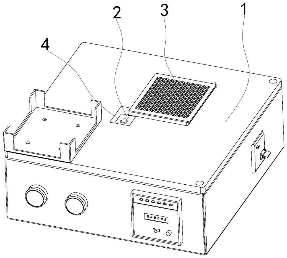
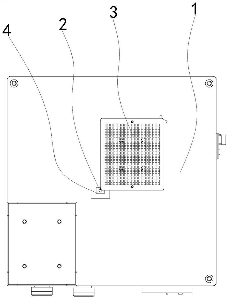
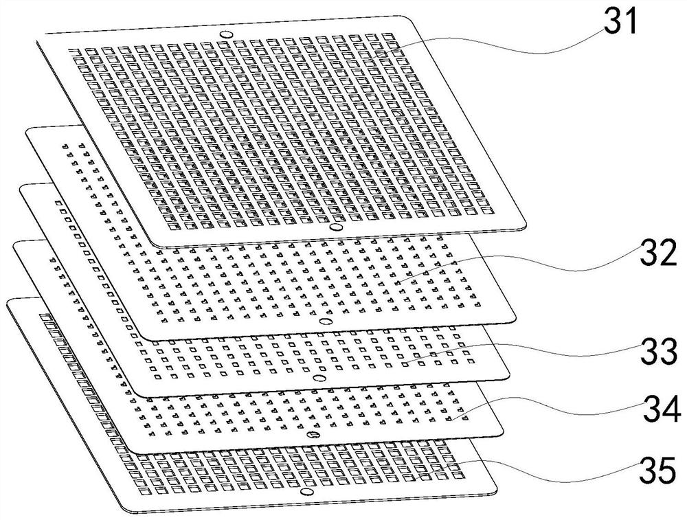
[0028] see Figure 1~4 , in the embodiment of the present invention, the coated wafer correction equipment includes a correction plate 3 for placing the wafer to be coated, and the correction plate 3 can be selected as a single-layer board or a multi-layer board according to actual production needs. In order to facilitate the subsequent sputtering coating, the correction plate 3 in this solution is a multi-layer plate. like image 3 As shown, the calibration...


PUM


Abstract

The invention discloses coated wafer correction equipment. The coated wafer correction equipment comprises a correction plate used for placing wafers to be coated and a lifting mechanism used for inclining the correction plate to enable the wafers to slide downwards along a plate body, the correction plate is provided with a positioning part located on the sliding track of the wafers, the positioning surface of the positioning part directly faces the wafers, and the wafers are tightly attached to the positioning surface of the positioning part in the sliding process. According to the coated wafer correction equipment, the wafers are arranged on the correction plate, and the plate body of the correction plate is inclined by arranging the lifting mechanism, so that the wafers slide down along the plate body and are tightly attached to the positioning part arranged opposite to the wafers in the sliding process, the distances among all the wafers are ensured to be fixed, and the coating positions on subsequent piezoelectric wafers are enabled to be the same.

Description

technical field [0001] The invention relates to the field of coating manufacturing, in particular to a coating wafer calibration device. Background technique [0002] The sputtering coating technology is to bombard the surface of the target with ions, and the phenomenon that the atoms of the target are knocked out is called sputtering. The deposition of atoms generated by sputtering on the surface of the substrate is called sputter coating. Usually, gas discharge is used to generate gas ionization, and its positive ions bombard the cathode target at high speed under the action of an electric field, knock out atoms or molecules of the cathode target, and fly to the surface of the substrate to be plated to form a thin film. [0003] When coating piezoelectric wafers, the piezoelectric wafers are placed on the calibration plate by an automated robotic arm. Due to the slight distance error during placement, the distances between all piezoelectric wafers may be different, result...

Claims


Application Information

Patent Timeline
IPC IPC(8): C23C14/50C23C14/34
CPCC23C14/34C23C14/50
Inventor 董书霞汤玉根汪鑫潘小龙
Owner HEFEI JINGWEITE ELECTRONICS CO LTD
Why Eureka
Try Eureka