Micro-LED test circuit, device and method

A technology for testing circuits and testing electrodes, which is applied in the directions of measuring devices, circuits, measuring electricity, etc., can solve the problems of low efficiency of wafer LED testing and so on.

Active Publication Date: 2021-04-09
CHENGDU VISTAR OPTEOLECTRONICS CO LTD
View PDF7 Cites 2 Cited by
  • Summary
  • Abstract
  • Description
  • Claims
  • Application Information

AI Technical Summary

Problems solved by technology

[0005] The present invention provides a Micro-LED test circuit, device and method to solve the problem of low efficiency of wafer LED testing and realize batch testing of wafer LEDs , which significantly improves the test efficiency

Method used


Image

  • Micro-LED test circuit, device and method
  • Micro-LED test circuit, device and method
  • Micro-LED test circuit, device and method

Examples


Embodiment 1

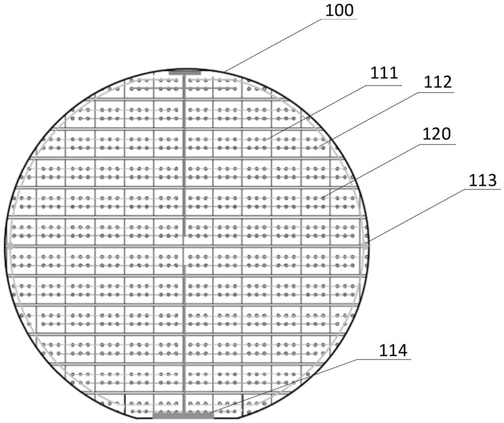
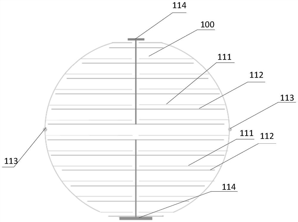
[0051] figure 1 It is a structural schematic diagram of an implementation mode of the Micro-LED test circuit in the embodiment of the present invention. Such as figure 1 As shown, the present embodiment provides a test circuit 100, including a first metal lead 111, a second metal lead 112, a first test electrode 113 and a second test electrode 114; the first metal lead 111 and the LED 120 of the wafer The anode is connected and extends to the outside of the epitaxial wafer or the light-emitting area of ​​the wafer; the second metal lead 112 is connected to the cathode of the LED 120 of the wafer, and extends to the outside of the epitaxial wafer or the light-emitting area of ​​the wafer; the first test electrode 113 is located on the extension section of the first metal lead 111; the second test electrode 114 is located on the extension section of the second metal lead 112; when the first test electrode 113 and the second test electrode 114 are respectively electrically conne...

Embodiment 2

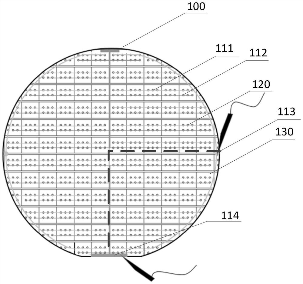
[0059] figure 2 It is a schematic structural diagram of another implementation of the Micro-LED test circuit in the embodiment of the present invention. Such as figure 2 As shown, the present embodiment provides a test circuit 100, including a first metal lead 111, a second metal lead 112, a first test electrode 113 and a second test electrode 114; the first metal lead 111 and the LED 120 of the wafer The anode is connected and extends to the outside of the epitaxial wafer or the light-emitting area of ​​the wafer; the second metal lead 112 is connected to the cathode of the LED 120 of the wafer, and extends to the outside of the epitaxial wafer or the light-emitting area of ​​the wafer; the first test electrode 113 is located on the extension section of the first metal lead 111; the second test electrode 114 is located on the extension section of the second metal lead 112; the first metal lead 111 and the second metal lead 112 divide the LED 120 of the wafer into two and ...

Embodiment 3

[0070] Figure 4 It is a structural schematic diagram of an implementation mode of the Micro-LED testing device in the embodiment of the present invention. Such as Figure 4 As shown, the present embodiment provides a test device 200, including: a stage 210, an image collector 220, a power supply 230, and a computer 240; The electrodes are contacted and connected to the second test electrodes, and are used to provide test signals to the LEDs of the wafer 250; the image collector 220 is used to collect test images corresponding to the wafer 250 during the test, and send the test images to the computer 240; the computer 240 A test result of the LEDs of the wafer 250 is obtained according to the test image.

[0071] In this embodiment, the wafer 250 has figure 1 , figure 2 In the shown test circuit, when testing, the wafer 250 is placed on the stage 210, and the probes connected to the power supply 230 or the test equipment are contacted with the first test electrode and the...


PUM


Abstract

The invention provides a Micro-LED test circuit, device and method. The test circuit comprises a first metal lead, a second metal lead, a first test electrode and a second test electrode. The first metal lead is connected with an anode of an LED of a wafer and extends to the outer side of an epitaxial wafer or a light-emitting area of the wafer; the second metal lead is connected with the cathode of the LED of the wafer and extends to the outer side of the epitaxial wafer or the light-emitting area of the wafer; the first test electrode is located on the extension section of the first metal lead; the second test electrode is positioned on the extension section of the second metal lead; and when the first test electrode and the second test electrode are electrically connected with external test equipment respectively, batch test is carried out on the LEDs of the wafer. According to the invention, the technical problem that the LED test efficiency of the wafer is low can be solved, batch test of wafer LEDs is realized, and the test efficiency is significantly improved.

Description

technical field [0001] The invention relates to a test circuit, device and method of Micro-LED, belonging to the technical field of organic light-emitting display. Background technique [0002] Micro-LED display technology has the advantages of high brightness, low power consumption, high resolution, high color saturation, and longer service life, so it is used in more and more display panels. In the manufacturing process of Micro-LED, performance testing of LED is required. [0003] The existing test method is to cover a glass cover plate on the top surface of the LED light source to fix the LED light source, and then use double probes to conduct electrical connection point test with the electrodes of the LED. [0004] However, the above test method is inefficient and not suitable for testing millions of LED chips on Micro-LED wafers. Contents of the invention [0005] The invention provides a Micro-LED testing circuit, device and method to solve the problem of low wafe...

Claims


Application Information

Patent Timeline
Patent Type & Authority Applications(China)
IPC IPC(8): H01L21/66G01R1/067G01R31/26
CPCH01L22/34H01L22/32G01R1/06705G01R31/2635
Inventor 田文亚郭恩卿王程功
Owner CHENGDU VISTAR OPTEOLECTRONICS CO LTD
Why Eureka
Try Eureka