Measuring method of metal film thickness on wafer surface

A surface metal and measurement method technology, which is applied in the direction of semiconductor/solid-state device testing/measurement, semiconductor devices, electrical components, etc., can solve the problems of increased plating time, reduced production capacity, increased cost, etc., and achieves high measurement accuracy and avoids Destruction, cost-saving effects

Active Publication Date: 2022-04-12
YANGTZE MEMORY TECH CO LTD
View PDF8 Cites 0 Cited by
  • Summary
  • Abstract
  • Description
  • Claims
  • Application Information

AI Technical Summary

Problems solved by technology

Since the thickness of the metal film cannot be monitored in real time before the metal grinding process, in order to make the thickness of the metal interconnection in the loose area and the dense area after the metal grinding process meet the requirements, the electroplating thickness will be increased when the metal is electroplated, and the thickness will be increased. , the electroplating time increases accordingly, the output rate of the electroplating equipment decreases, the material consumption increases, and the cost increases; at the same time, the thickness of the electroplating increases, and in the subsequent metal grinding process, the output rate of the metal grinding equipment decreases, the amount of grinding fluid used increases, and the production capacity decreases. cost increase

Method used


Image

  • Measuring method of metal film thickness on wafer surface
  • Measuring method of metal film thickness on wafer surface
  • Measuring method of metal film thickness on wafer surface

Examples


Embodiment Construction

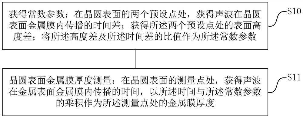
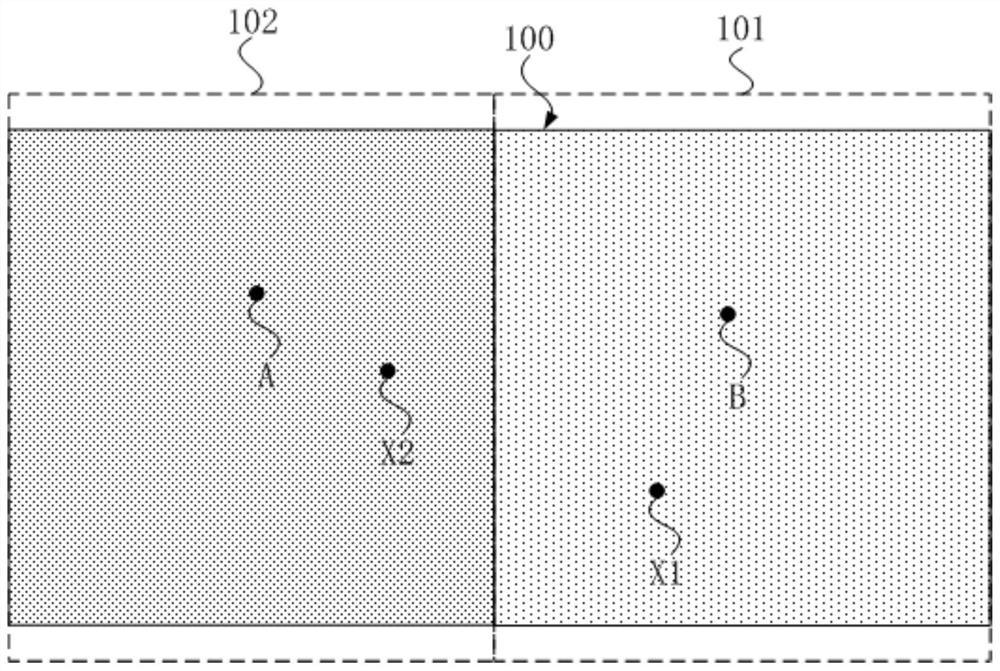
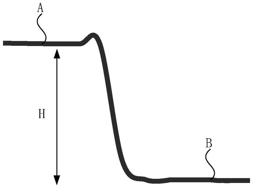
[0027] The specific implementation of the method for measuring the thickness of the metal film on the wafer surface provided by the present invention will be described in detail below in conjunction with the accompanying drawings.

[0028] As mentioned in the background art, there is no real-time means for monitoring the thickness of the metal film at the metal coating process site. It is usually necessary to measure the thickness of the metal layer after the metal grinding process, which fails to achieve the purpose of real-time monitoring, and in order to make the thickness of the metal interconnection line in the loose area and the dense area after the metal grinding process meet the requirements, when electroplating metal It will increase the plating thickness, resulting in reduced production capacity and increased costs.

[0029] Therefore, the present invention provides a method for measuring the thickness of the metal film on the surface of the wafer, which can monitor ...


PUM


Abstract

The invention provides a method for measuring the thickness of a metal film on the surface of a wafer, which includes the following steps: Obtaining constant parameters: at two preset points on the surface of the wafer, obtaining the time difference of sound waves propagating in the metal film on the surface of the wafer; obtaining the obtained The surface height difference at the two preset points; the ratio of the height difference and the time difference is used as the constant parameter; the thickness measurement of the metal film on the wafer surface: at the measurement point on the wafer surface, the sound wave is obtained in the crystal The time of propagation in the metal film on the circular surface, the product of the time and the constant parameter is taken as the thickness of the metal film at the measurement point. The measurement method of the present invention can monitor the thickness of the metal film on the surface of the wafer in real time, and has high measurement accuracy, which greatly improves the productivity and saves the cost; moreover, the surface height difference at two preset points can be obtained without destroying the wafer, Avoid wafer damage and provide a non-destructive measurement method.

Description

technical field [0001] The invention relates to the technical field of semiconductors, in particular to a method for measuring the thickness of a metal film on a wafer surface. Background technique [0002] During the wafer production process, various film layers, including metal films, are formed on the surface. Among them, in the metal electroplating process for forming the metal film, the metal growth rate of the dense region and the loose region of the base structure differs greatly. The thickness of the dense region is more than twice the thickness of the loose region, which poses a great challenge to the subsequent metal grinding process. If the difference in the thickness of the metal film in the dense area and the loose area of ​​the wafer is too large, the metal film on the surface of the loose area has been completely ground off during the metal grinding process, while the metal film on the surface of the dense area has not been removed. There are still metal res...

Claims


Application Information

Patent Timeline
Patent Type & Authority Patents(China)
IPC IPC(8): H01L21/66H01L21/768
CPCH01L22/12H01L21/76838H01L2221/1068
Inventor 李辉梅双
Owner YANGTZE MEMORY TECH CO LTD
Why Eureka
Try Eureka