

Cutting method of large-size silicon wafer
A cutting method, large-scale technology, applied in the field of solar energy, can solve problems such as high cost
- Summary
- Abstract
- Description
- Claims
- Application Information
AI Technical Summary
Problems solved by technology
Method used
Image

Examples
Embodiment 1
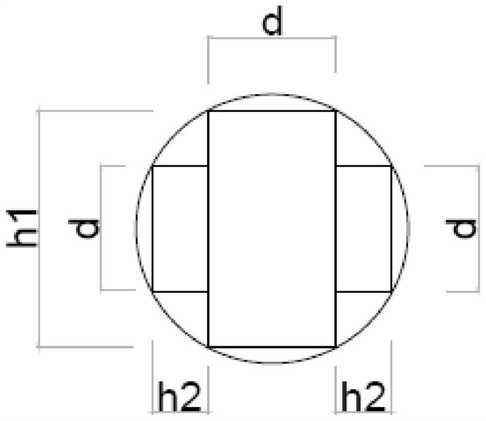
[0024] Single-wafer rods are obtained by the Czochralski method, and the heads and tails of the single-wafer rods are removed, such as figure 1 As shown, when the effective diameter of the single wafer rod is greater than one time of the target silicon wafer width d and less than or equal to three times the target silicon wafer width d, the round rod is cut into three cubic square rods, and the larger cubic crystal The length of one side of the rod is d, the length of the other side is h1, the depth of the cube along the longitudinal axis of the ingot is l, and the other two relatively small cubes, the length of one side is d, the length of the other side is h2, and the cube is along the longitudinal axis of the ingot The depth in the direction is l, and the whole silicon round rod is cut into three cubic ingots with length l in the longitudinal direction. After the cubic ingot is prepared, it is cut into rectangular silicon wafers along the side lengths h1 and h2, where the w...
Embodiment 2
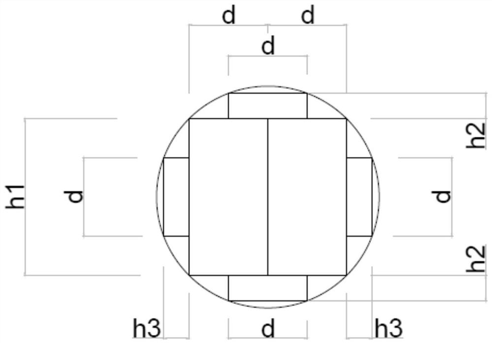
[0026] When the effective diameter of the single wafer rod is greater than twice the target silicon wafer width d and less than three times the target silicon wafer width d, the single wafer rod is obtained by the Czochralski method, and the head and tail of the single wafer rod are removed, such as figure 2 As shown, the single wafer rod is cut longitudinally along the axial direction, and the round rod is cut into 6 cubic crystal rods, of which 2 larger cubic crystal rods have one side with a length of d and one side with a length of h1, and the cube is along the The depth in the direction of the longitudinal axis of the ingot is l; the other two relatively small cubes have a length of d on one side and a length of h2 on the other side, and the depth of the cube along the longitudinal axis of the single wafer rod is l; there are two other relatively small cubes A cube with one side length d and one side length h3, the depth of the cube along the longitudinal axis of the sing...
Embodiment 3
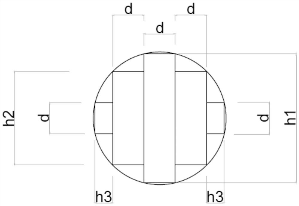
[0028] A single wafer rod is obtained by the Czochralski method, and the head and tail of the single wafer rod are removed. When the effective diameter of the single wafer rod is greater than three times the width d of the target silicon wafer, such as image 3 As shown, the round rod is cut into 5 cubic crystal rods, one of which has a dimension of one side length d and one side length h1, and the depth of the cube along the longitudinal axis of the single wafer rod is l; The length is d, the length of one side is h2, the depth of the cube along the longitudinal axis of the ingot is l; the length of the remaining two sides is d, the length of one side is h3, and the depth of the cube along the longitudinal axis of the ingot is l; The silicon round rod is cut into five cubes with a length l in the longitudinal direction. After the cubic crystal ingot is prepared, it is cut into rectangular silicon wafers along the sides with lengths of h1, h2 and h3 respectively, wherein the w...
PUM
| Property | Measurement | Unit |
|---|---|---|
| Thickness | aaaaa | aaaaa |
| Thickness | aaaaa | aaaaa |
| Thickness | aaaaa | aaaaa |
Abstract
Description
Claims
Application Information