Three-dimensional flash memory including intermediate wiring layer, and manufacturing method therefor

A flash memory, three-dimensional technology, applied in static memory, read-only memory, semiconductor/solid-state device manufacturing, etc., can solve the problems of high process cost and material degradation, and achieve simplified wiring process, improved integration, and reduced unit The effect of deterioration of characteristics

Pending Publication Date: 2021-04-13
SAMSUNG ELECTRONICS CO LTD
View PDF0 Cites 0 Cited by
  • Summary
  • Abstract
  • Description
  • Claims
  • Application Information

AI Technical Summary

Problems solved by technology

[0019] Embodiments propose a method of manufacturing a three-dimensional flash memory, in which at least one intermediate wiring layer is formed using a back-end process, thereby overcoming the problem of material degradation of a conventional manufacturing technique of forming at least one intermediate wiring layer before forming an upper string And the disadvantage of high process cost

Method used


Image

  • Three-dimensional flash memory including intermediate wiring layer, and manufacturing method therefor
  • Three-dimensional flash memory including intermediate wiring layer, and manufacturing method therefor
  • Three-dimensional flash memory including intermediate wiring layer, and manufacturing method therefor

Examples


Embodiment Construction

[0090] Hereinafter, embodiments will be described in detail with reference to the accompanying drawings. However, the present invention is not limited or restricted by the examples. In addition, the same reference numerals shown in each drawing designate the same elements.

[0091] In addition, terms used herein may be terms for appropriately expressing preferred embodiments of the present invention, and may be changed based on user's or operator's intention or custom of those of ordinary skill in the art. Therefore, definitions of terms must be determined based on the contents described in the specification.

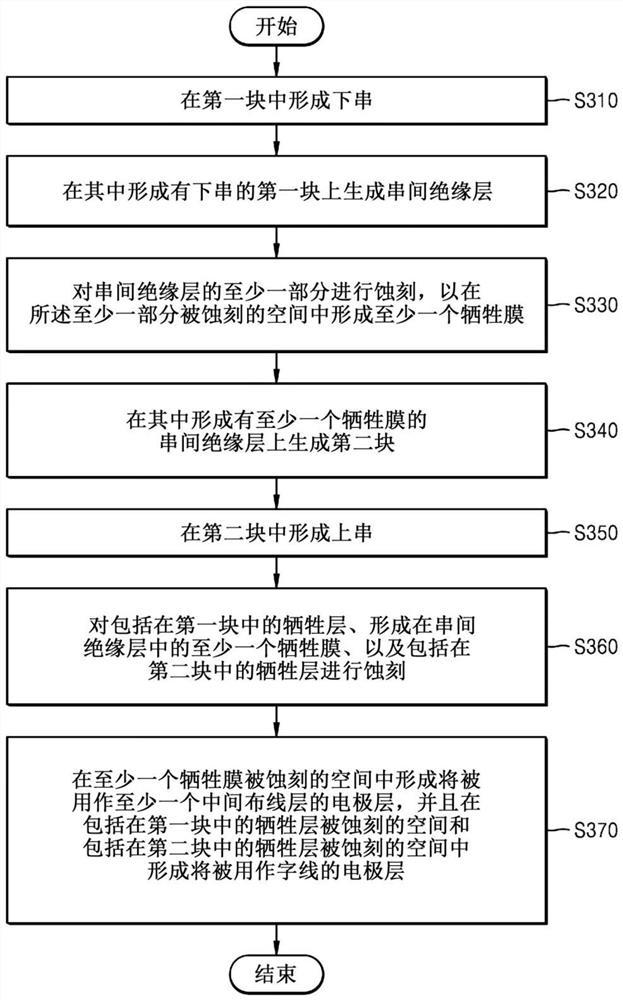
[0092] image 3 is a flowchart illustrating a method of manufacturing a three-dimensional flash memory according to an embodiment, Figure 4A to Figure 4J is shown for description image 3 A diagram of a first embodiment of a method of fabricating a three-dimensional flash memory is shown. Hereinafter, it is assumed that the method of manufacturing a three-dimensio...


PUM


Abstract

A three-dimensional flash memory including an intermediate wiring layer, and a manufacturing method therefor are disclosed. According to one embodiment, a method for manufacturing a three-dimensional flash memory by using a post process comprises the steps of: forming a lower string at a first block, which includes a sacrificial layer and an insulating layer that extend in a first direction so as to be alternately stacked; generating an inter-string insulating film in the upper region of the first block having the lower string; etching at least a part of the inter-string insulating film so as to form at least one sacrificial film in the space in which the at least a part of the inter-string insulating film is etched; generating, in the upper region of the inter-string insulating film having the at least one sacrificial film, a second block, which includes the sacrificial layer and the insulating layer that extend in the first direction so as to be alternately stacked; forming an upper string at the second block; etching the sacrificial layer included in the first block, the at least one sacrificial film, and the sacrificial layer included in the second block; and forming an electrode layer to be used as at least one intermediate wiring layer in the space in which the at least one sacrificial film is etched, and an electrode layer used as a word line in the space in which the sacrificial layer included in the first block is etched and in the space in which the sacrificial layer included in the second block is etched.

Description

technical field [0001] The following embodiments relate to methods of manufacturing a three-dimensional flash memory, and more particularly, to a three-dimensional flash memory including an intermediate wiring layer. Background technique [0002] The flash memory device can be electrically erasable and programmable electrically erasable programmable read-only memory (EEPROM), and this memory is commonly used in computers, digital cameras, MP3 players, game systems, memory sticks, etc. . The flash memory device electrically controls input / output of data through Fowler-Nordheim (F-N) tunneling or hot electron injection. [0003] In detail, refer to the article showing the array of the related art three-dimensional flash memory figure 1 , the array of the three-dimensional flash memory may include a common source line CSL, a bit line BL, and a plurality of cell strings CSTR arranged between the common source line CSL and the bit line BL. [0004] The bit lines are two-dimens...

Claims


Application Information

Patent Timeline
Patent Type & Authority Applications(China)
IPC IPC(8): H01L27/11551H01L27/11521H01L27/11578H01L27/11568H01L29/423H01L29/66H01L29/788H01L21/311H01L27/11556H01L27/11524
CPCG11C16/0483G11C16/26H10B43/10H10B43/27H01L23/5283H10B41/10H10B41/27H10B41/30H10B43/30
Inventor 宋润洽
Owner SAMSUNG ELECTRONICS CO LTD
Why Eureka
Try Eureka