
Patsnap Eureka
For R&D, Patsnap Eureka makes reading and utilizing patents & technical documents easy.
Patsnap Eureka AIR
Designed for self-driven R&D workflows. Generate viable solutions, solve complex R&D challenges, empower your innovation with AI.

Patsnap Eureka Materials
Designed for material experts only. Revolutionize your material R&D, from search, analyze, to developing new materials.

TechResearch
Generate reliable direction feasibility study reports for your R&D in just a few steps.

TechSeek
Discover and master advanced knowledge NOW. Basics, ideas, possibilities, all at once.

TechMind
As an expert in R&D Theories, TechMind can generates customized viable solutions instantly.

TechRisk
Analyze your overall solution with one click, know your potential R&D risks in advance.

TechMonitor
Get weekly tech updates, stay abreast of the latest tech innovations and key insights.
Wafer detection method
A detection method and wafer technology, applied in the direction of semiconductor/solid-state device testing/measurement, can solve problems such as disadvantages, improve process yield, etc., and achieve the effect of improving yield
- Summary
- Abstract
- Description
- Claims
- Application Information
AI Technical Summary
Problems solved by technology
Method used
Image

Examples
no. 1 approach
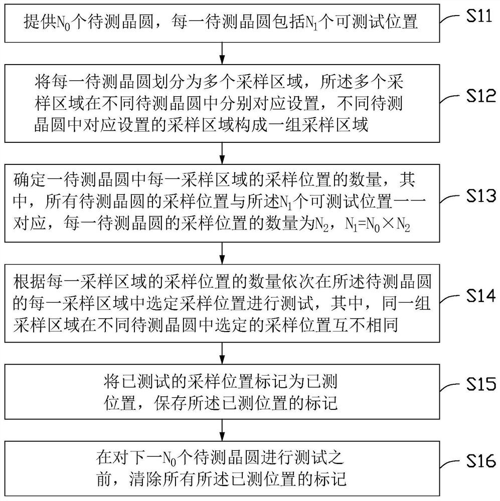
[0034] see figure 1 , the first embodiment of the present invention provides a wafer detection method, including the following steps:
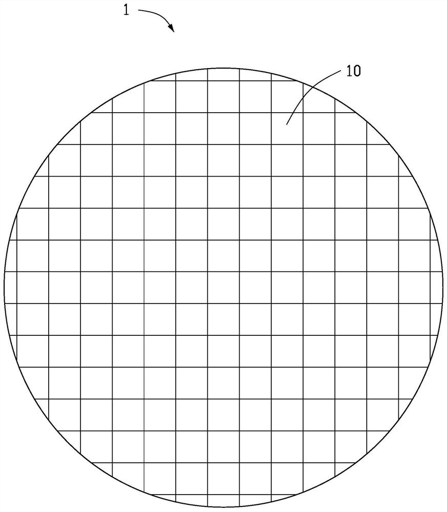
[0035] Step S11, please also refer to figure 2 , providing N 0 Wafers 1 to be tested, each wafer 1 to be tested includes N 1 10 testable locations.
[0036] For example, the number of wafers 1 to be tested is 20 (ie N 0 =20). Each wafer 1 to be tested includes 160 testable positions 10 (ie N 1 =160).
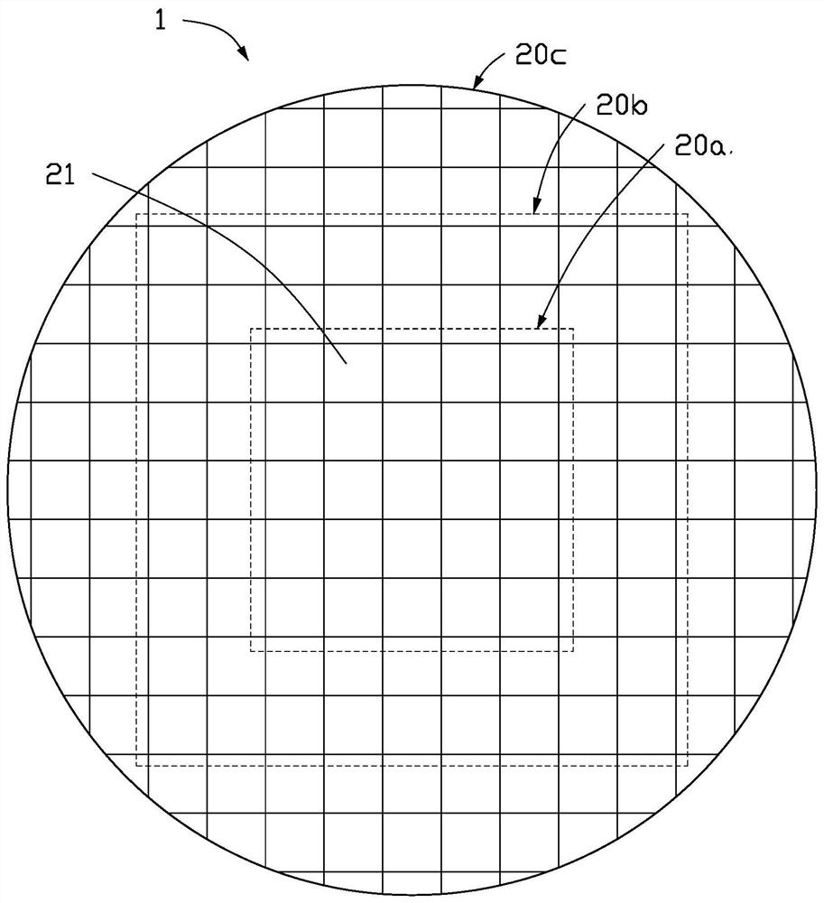
[0037] Step S12, please also refer to image 3 , divide each wafer 1 to be tested into a plurality of sampling areas according to a predetermined division method, the plurality of sampling areas are correspondingly set in different wafers 1 to be tested, and the sampling areas correspondingly set in different wafers 1 to be tested are Regions form a set of sampling regions.
[0038] As shown in the figure, each wafer 1 to be tested may include three sampling areas, respectively marked as a first sampling area 20a, a second sampling are...
no. 2 approach
[0059] see Figure 7 , the second embodiment of the present invention also provides a wafer detection method, including the following steps:
[0060] Step S71, please also refer to figure 2 , providing N 0 Wafers 1 to be tested, each wafer 1 to be tested includes N 1 10 testable locations.
[0061] For example, the number of wafers 1 to be tested is 40 (ie N 0 = 40). Each wafer 1 to be tested includes 160 testable positions 10 (ie N 1 =160).
[0062] Step S72, please refer to image 3 , divide each wafer 1 to be tested into a plurality of sampling areas according to a predetermined division method, the plurality of sampling areas are correspondingly set in different wafers 1 to be tested, and the sampling areas correspondingly set in different wafers 1 to be tested are Regions form a set of sampling regions.
[0063] As shown in the figure, each wafer 1 to be tested may include three sampling areas, respectively marked as a first sampling area 20a, a second sampling ...
PUM
 Abstract
Description
Claims
Application Information
 - R&D Engineer
- R&D Manager
- IP Professional
- Industry Leading Data Capabilities
- Powerful AI technology
- Patent DNA Extraction
Browse by: Latest US Patents, China's latest patents, Technical Efficacy Thesaurus, Application Domain, Technology Topic, Popular Technical Reports.
© 2024 PatSnap. All rights reserved.Legal|Privacy policy|Modern Slavery Act Transparency Statement|Sitemap|About US| Contact US: help@patsnap.com