Optical sensor, preparation method thereof and display panel

A light sensor, yellow light process technology, applied in the display field, can solve the problem of limiting the signal-to-noise ratio of weak light detection, and achieve the effects of high signal-to-noise ratio, high light response, and cost reduction

Active Publication Date: 2021-04-16
TCL CHINA STAR OPTOELECTRONICS TECH CO LTD
View PDF11 Cites 4 Cited by
  • Summary
  • Abstract
  • Description
  • Claims
  • Application Information

AI Technical Summary

Problems solved by technology

[0005] The optical sensor and its preparation method and display panel provided by the present invention solve the problem that when the 2T1C structure is used as the optical sensor matrix unit in the existing optical sensor, the signal size at the reading end of the switch TFT depends on the optical response of the a-Si TFT, thereby limiting Solved the technical problems of light sensor's detection of weak light and signal-to-noise ratio

Method used


Image

  • Optical sensor, preparation method thereof and display panel
  • Optical sensor, preparation method thereof and display panel
  • Optical sensor, preparation method thereof and display panel

Examples


Embodiment Construction

[0043] The following descriptions of the various embodiments refer to the accompanying drawings to illustrate specific embodiments in which the invention may be practiced. The directional terms mentioned in the present invention, such as [top], [bottom], [front], [back], [left], [right], [inside], [outside], [side], etc., are only for reference The orientation of the attached schema. Therefore, the directional terms used are used to illustrate and understand the present invention, but not to limit the present invention. In the figures, structurally similar elements are denoted by the same reference numerals.

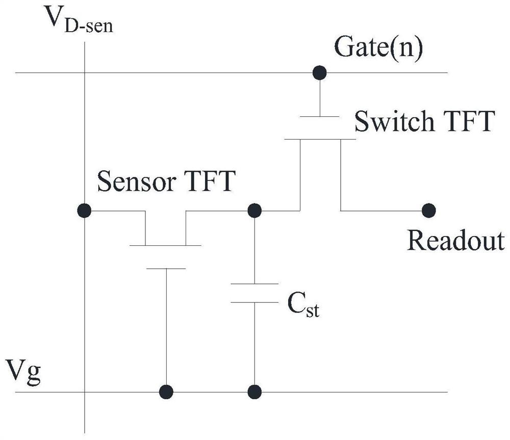
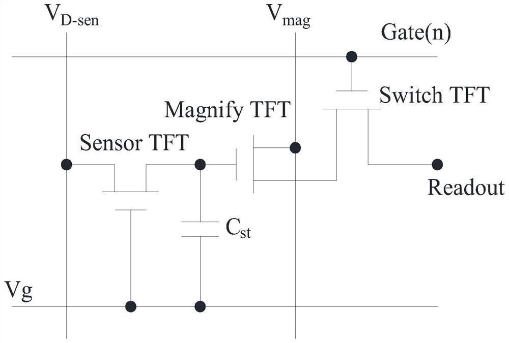
[0044] In the present invention, when the optical sensor matrix unit of the display panel in the prior art adopts a 2T1C structure, the signal size of the switch TFT reading end depends on the optical response of the a-Si TFT, thereby limiting the detection of weak light and signal noise of the optical sensor However, this embodiment can solve this defect.

[0045] Plea...


PUM


Abstract

The invention provides an optical sensor, a manufacturing method thereof and a display panel. The optical sensor comprises a plurality of optical sensor matrix units, and each optical sensor matrix unit comprises an induction TFT, an amplification TFT, a switch TFT and a storage capacitor, wherein an active layer of the induction TFT is amorphous silicon, an active layer of the amplification TFT is an oxide semiconductor, the induction TFT is connected with the amplification TFT, the amplification TFT is connected with the switch TFT, the switch TFT controls reading of electric signals detected by the induction TFT and amplified by the amplifying TFT, and when the amplification TFT is in an on state, the electric signals are transmitted to the signal reading circuit. A 3T1C architecture is adopted as an optical sensor matrix unit to replace a traditional 2T1C architecture, detection of weak light by an optical sensor can be achieved, the optical response of the optical sensor is effectively improved, and the optical sensor has high optical response and a high signal-to-noise ratio; the preparation of the induction TFT and the amplification TFT shares a plurality of yellow light processes, so the cost is reduced, and the advantages of large area and high uniformity of aSi can be fully exerted.

Description

technical field [0001] The invention relates to the field of display technology, in particular to an optical sensor, a preparation method thereof, and a display panel. Background technique [0002] With the rapid development of display panels in electronic products such as mobile phones, TVs, tablets, and smart watches, people's pursuit of smart displays is also getting higher and higher. Integrated light sensors rely on their advantages in remote light interaction, gesture sensing, Applications in fields such as ambient light sensing and personal identification are expected to realize a new type of smart display with multiple functions. [0003] Optical sensors based on amorphous silicon (a-Si) thin film transistors (Thin Film Transistor, TFT) have the advantages of mature technology, high uniformity in large areas, low cost, high responsivity, high signal-to-noise ratio, and small size. has received widespread attention. Please refer to figure 1 , the traditional a-Si T...

Claims


Application Information

Patent Timeline
Patent Type & Authority Applications(China)
IPC IPC(8): H01L27/12H01L21/77G09F9/33G09F9/35G02F1/1333
CPCY02P70/50
Inventor 蔡广烁郭力
Owner TCL CHINA STAR OPTOELECTRONICS TECH CO LTD
Why Eureka
Try Eureka