Semiconductor device and preparation method thereof
A technology for semiconductors and devices, applied in the field of semiconductor devices and their preparation, can solve the problems of reducing the resistance uniformity of resistive memory, reducing the reliability of resistive memory, and inability to apply computing, etc.
- Summary
- Abstract
- Description
- Claims
- Application Information
AI Technical Summary
Problems solved by technology
Method used
Image

Examples
preparation example Construction
[0065] Another embodiment of the present invention also provides a method for preparing a semiconductor device, such as Figure 8 shown, including:
[0066] Step S401: Depositing a bottom electrode layer material on a semiconductor substrate to form a bottom electrode layer, the bottom electrode layer having a bottom electrode perpendicular to the upper surface of the semiconductor substrate;
[0067] Step S402: Depositing a resistive variable layer material and a top electrode material on the bottom electrode layer, and patterning the resistive variable layer material and top electrode material to form a resistive variable layer and a top electrode.
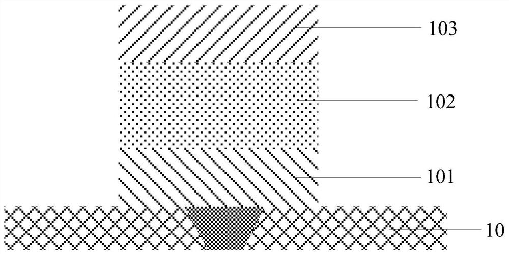
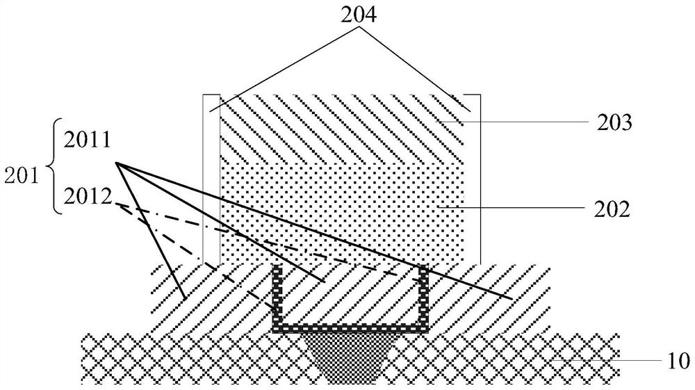
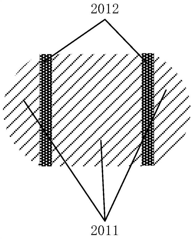
[0068] Step S403: Deposit an oxygen barrier protective layer material on the surface of the resistive switch layer and the top electrode, and etch the oxygen barrier protective layer material by using a sidewall etching method to form a layer covering the resistive switch layer and the sidewall of the top electrode oxygen barri...
PUM
 Abstract
Description
Claims
Application Information
 - R&D
- Intellectual Property
- Life Sciences
- Materials
- Tech Scout
- Unparalleled Data Quality
- Higher Quality Content
- 60% Fewer Hallucinations
Browse by: Latest US Patents, China's latest patents, Technical Efficacy Thesaurus, Application Domain, Technology Topic, Popular Technical Reports.
© 2025 PatSnap. All rights reserved.Legal|Privacy policy|Modern Slavery Act Transparency Statement|Sitemap|About US| Contact US: help@patsnap.com