Device transfer method

A transfer method and device technology, which can be used in the manufacture of electrical solid-state devices, semiconductor devices, semiconductor/solid-state devices, etc., can solve problems such as yield problems, and achieve the effects of reducing costs, improving transfer yield, and improving device transfer efficiency.

Pending Publication Date: 2021-04-23
GUANGDONG INST OF SEMICON IND TECH
View PDF7 Cites 3 Cited by
  • Summary
  • Abstract
  • Description
  • Claims
  • Application Information

AI Technical Summary

Problems solved by technology

[0002] Currently, there is no mature and commercial mass transfer technology route. The existing organic stamp technology, roll-to-roll technology, fluid assembly technology, etc. all have their own technical shortcomings, such as yield problems or efficiency problems.

Method used


Image

  • Device transfer method
  • Device transfer method
  • Device transfer method

Examples


Embodiment

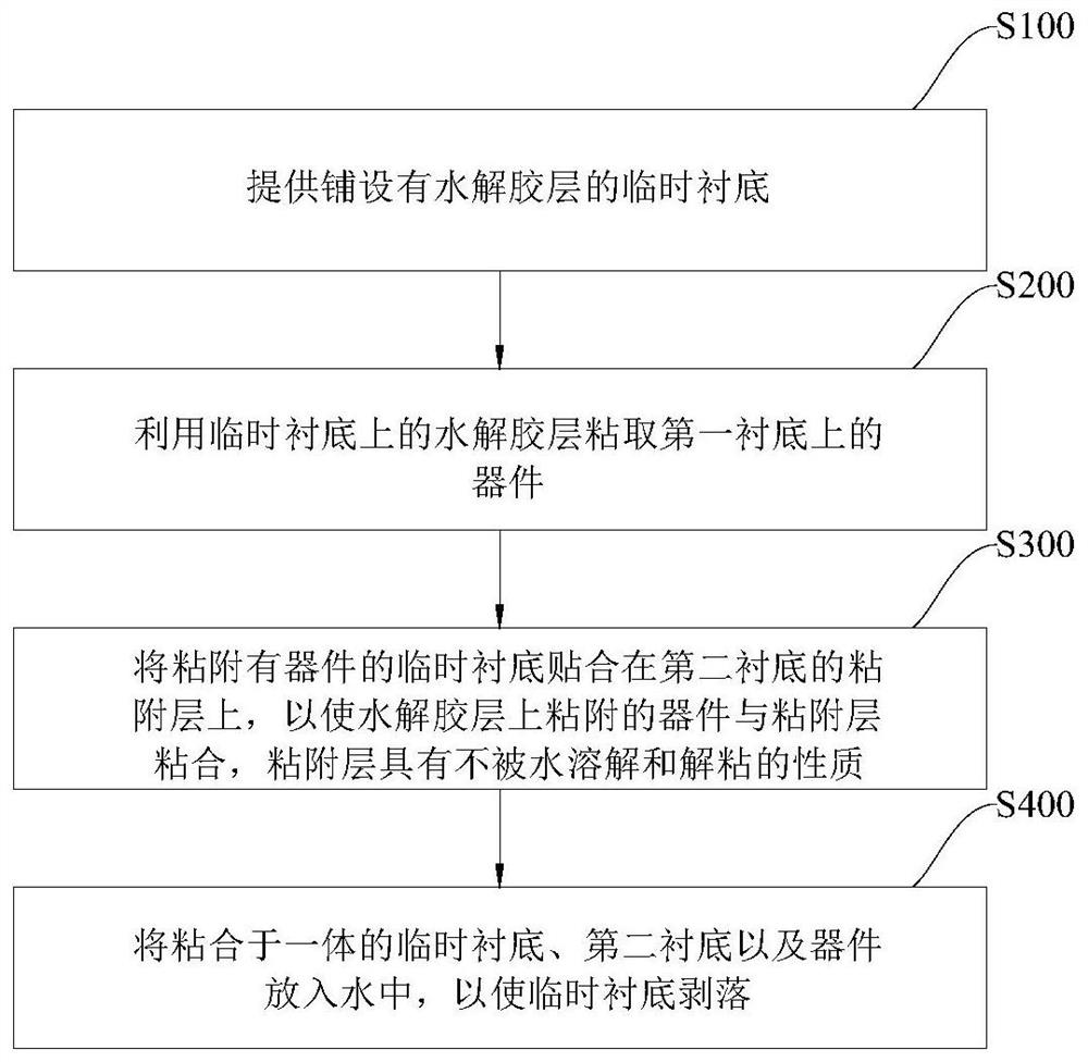
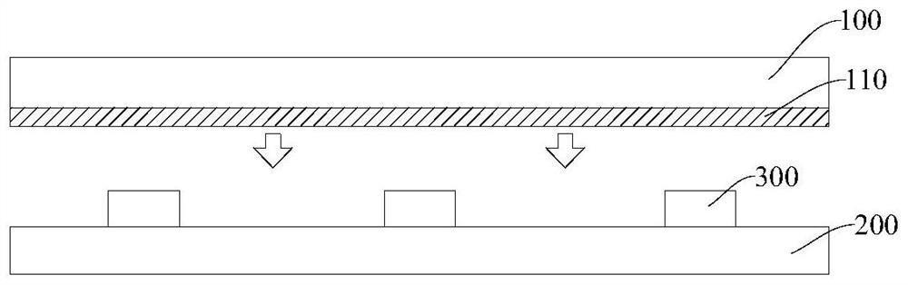
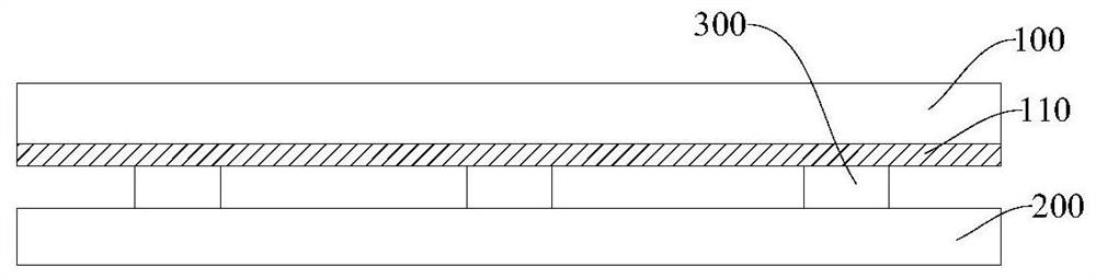
[0043] figure 1 It is a flowchart of a device 300 transfer method in an embodiment of the present application; Figure 2 to Figure 7 It is a schematic diagram of the transfer process of the device 300 in an embodiment of the present application. Please refer to figure 1 and Figure 7 , the device 300 transfer method provided by the embodiment of the present application includes:

[0044] Step S100, providing a temporary substrate covered with a hydrolytic glue layer.

[0045] In an optional embodiment of the present application, the temporary substrate 100 may be a rigid or flexible substrate, and its material includes but is not limited to glass, sapphire, polyester resin (Polyethylene terephthalate, PET) or polyimide resin (Polymide, PI). In this embodiment, the temporary substrate 100 may be flat, and the hydrolytic glue layer 110 is evenly laid on one side of the temporary substrate 100 as a transfer adhesive.

[0046] Specifically, in this embodiment, the hydrolytic...


PUM


Abstract

The invention discloses a device transfer method, and relates to the technical field of semiconductors. According to the device transfer method provided by the invention, a device on a first substrate is bonded off by using a hydrolytic adhesive layer, and then the bonded device is bonded on the adhesive layer of a second substrate, so that the device bonded on the hydrolytic adhesive layer is bonded with the adhesive layer, and the adhesive layer has the property of being not dissolved and debonded by water. And finally, a temporary substrate, the second substrate and the device which are bonded into a whole are put into water, the hydrolytic adhesive layer is disssolved in water, and the temporary substrate is peeled off to obtain the second substrate to which the device is bonded, thereby completing the transfer of the device. According to the device transfer method provided by the invention, the hydrolytic adhesive is used as a transfer adhesive and can be completely removed after transfer, so that the problem that part of devices are left on the temporary substrate is solved, and the transfer yield is improved. And the hydrolytic adhesive can be applied to the temporary substrate in a large area coating manner, and large-area and large-quantity transfer can be realized, so that the transfer efficiency of the device is improved.

Description

technical field [0001] The present application relates to the field of semiconductor technology, in particular, to a device transfer method. Background technique [0002] At present, there is no mature and commercial mass transfer technology route. The existing organic stamp technology, roll-to-roll technology, fluid assembly technology, etc. all have their own technical shortcomings, such as yield problems or efficiency problems. [0003] In view of this, the present application is proposed. Contents of the invention [0004] The purpose of the present application is to provide a device transfer method, which can improve the device transfer yield and transfer efficiency. [0005] This application is implemented like this: [0006] In a first aspect, the present application provides a device transfer method, including: [0007] Provide a temporary substrate with a hydrolytic adhesive layer; [0008] taking the device on the first substrate by using the hydrolytic glue ...

Claims


Application Information

Patent Timeline
Patent Type & Authority Applications(China)
IPC IPC(8): H01L21/683
CPCH01L21/6836H01L2221/68368
Inventor 潘章旭龚政郭婵龚岩芬刘久澄王建太胡诗犇庞超陈志涛
Owner GUANGDONG INST OF SEMICON IND TECH
Why Eureka
Try Eureka