Chip peripheral anti-fuse pre-trimming circuit and trimming method thereof

An anti-fuse and pre-repair technology, applied in logic circuits, adjusting electrical variables, electrical components, etc., can solve the problems of long production test time and low efficiency, achieve improved repair efficiency, good process compatibility, and reduce production The effect of testing costs

Active Publication Date: 2021-04-23
QX MICRO DEVICES
View PDF6 Cites 6 Cited by
  • Summary
  • Abstract
  • Description
  • Claims
  • Application Information

AI Technical Summary

Problems solved by technology

The disadvantage of this trimming method is that in the pre-trimming process, all possible antifuse combinations must be tested once. When there are many antifuse bits, the production test time is long and the efficiency is low. If there are n bits of antifuse bits , you need to test 2 n values, for example, when the antifuse bits have 10 bits, 1024 values ​​need to be tested

Method used


Image

  • Chip peripheral anti-fuse pre-trimming circuit and trimming method thereof
  • Chip peripheral anti-fuse pre-trimming circuit and trimming method thereof
  • Chip peripheral anti-fuse pre-trimming circuit and trimming method thereof

Examples


Embodiment Construction

[0055] The present invention will be described in further detail below in conjunction with accompanying drawing:

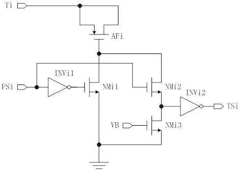
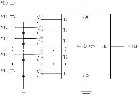
[0056] image 3 An embodiment of the chip peripheral pre-trimming circuit of the present invention is shown.

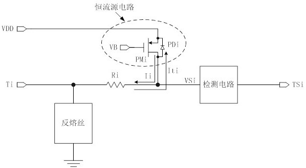
[0057] see image 3 As shown, the anti-fuse pre-trimming circuit on the periphery of the chip includes an integrated circuit, and the integrated circuit has an n-bit anti-fuse trimming circuit and a first melting voltage Ti (i=1,2,3,... ,n) one-to-one correspondence, the switches Si (i=1,2,3,…,n) are respectively connected to the pins of the first fusing voltage Ti (i=1,2,3,…,n) of the integrated circuit above; among them, VDD is the power supply voltage pin of the integrated circuit; VSS is the ground pin of the integrated circuit; TEP is the output pin of the modified electric parameter. The switch Si (i=1, 2, 3,..., n) can be a MOSFET switch tube, a BJT switch tube, or a switching device such as a relay, or a combination of these switching devices. ...


PUM


Abstract

The invention relates to a chip peripheral anti-fuse pre-trimming circuit and a trimming method thereof. The trimming method comprises the following steps: calculating a rough pre-trimming value by using a formula according to an electrical parameter initial value and an electrical parameter target value which are tested before melting, and converting to obtain a rough pre-trimmed anti-fuse combination; according to the rough pre-trimming anti-fuse combination, carrying out the rough virtual fusion burning on the anti-fuse, and testing a rough electrical parameter value; calculating a pre-trimming value deviation by using the designed trimming step length of the electrical parameter, the rough electrical parameter value and the electrical parameter target value; determining an accurate pre-trimming range according to the pre-trimming value deviation, performing virtual fusion burning on the anti-fuse according to each anti-fuse trimming combination in the accurate pre-trimming range, testing a corresponding electrical parameter pre-trimming value, and obtaining an accurate anti-fuse combination when the tested electrical parameter value is closest to a target value under a certain anti-fuse combination; carrying out fusion burning on the antifuse according to the precise antifuse combination, and testing and verifying whether an error between the final value and the target value of the electrical parameter meets the requirement or not.

Description

technical field [0001] The invention belongs to the technical field of integrated circuits, and in particular relates to a chip peripheral anti-fuse pre-adjustment circuit and a trimming method for implementing anti-fuse with a CMOS low-voltage process. Background technique [0002] Anti-fuse usually refers to this type of device and circuit that is melted by a certain voltage or current to irreversibly change from the original open circuit state to a short circuit state. It is generally used to adjust certain electrical parameters in the circuit, such as: reference voltage, frequency, etc. [0003] The anti-fuse trimming circuit is a circuit for melting and detecting the anti-fuse. In addition to ensuring reliable and stable melting of the anti-fuse, the anti-fuse trimming circuit must also ensure that the integrated circuit Other devices and circuits in the circuit will not be damaged, and at the same time, it is necessary to detect the open and short-circuit states of th...

Claims


Application Information

Patent Timeline
Patent Type & Authority Applications(China)
IPC IPC(8): H03K19/00H03K19/094G05F1/56
CPCG05F1/56H03K19/0005H03K19/0941
Inventor 毛晓峰黄朝刚李剑
Owner QX MICRO DEVICES
Why Eureka
Try Eureka