Clock detection circuit and method

A clock detection, circuit technology, applied in electrical components, pulse processing, pulse technology, etc.

Pending Publication Date: 2021-04-27
GREE ELECTRIC APPLIANCES INC +1
View PDF0 Cites 0 Cited by
  • Summary
  • Abstract
  • Description
  • Claims
  • Application Information

AI Technical Summary

Problems solved by technology

[0005] In order to solve the limitations caused by the external high-frequency clock to de

Method used


Image

  • Clock detection circuit and method
  • Clock detection circuit and method
  • Clock detection circuit and method

Examples


Embodiment 1

[0074] At present, in the prior art, the burrs in the clock signal are generally eliminated by D flip-flops, and the characteristics of the D flip-flops being insensitive to burrs are used to eliminate them, but the existing methods are not thorough in eliminating burrs. A deburring unit 3 is provided;

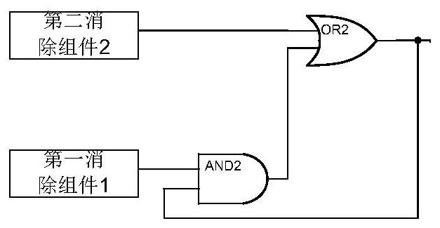
[0075] Such as figure 1 As shown, the burr elimination unit 3 includes a primary elimination unit and a secondary elimination unit, and the secondary elimination unit includes a first OR gate and a first AND gate, wherein,

[0076] The primary elimination unit includes a first elimination component 1 and a second elimination component 2;

[0077] The first elimination component 1 is used to eliminate low burrs in the clock signal to be tested;

[0078] The second elimination component 2 is used to eliminate high burrs in the clock signal to be tested;

[0079] One input end of the first AND gate is connected to the output end of the first elimination component 1, and the ot...

Embodiment 2

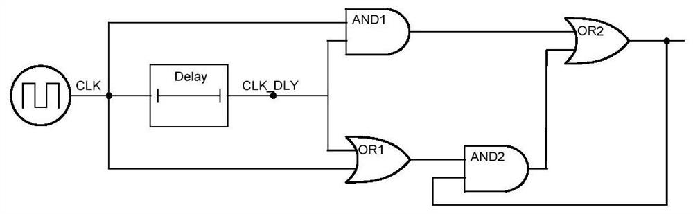
[0089] Embodiment 2 includes all the content in Embodiment 1, and will not be repeated here, wherein the first elimination component 1 includes a second OR gate and a delayer,

[0090] The input end of the delayer is connected to the clock 7 to be tested, and the output end of the delayer is connected to an input end of the second OR gate;

[0091] The other input end of the second OR gate is connected to the clock 7 to be tested;

[0092] An output end of the second OR gate is connected to an input end of the first AND gate.

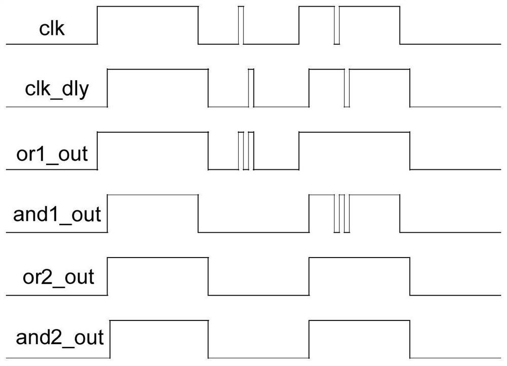
[0093] In this embodiment, the two input terminals of the second OR gate respectively input the clock signal to be tested and the delayed signal, and low glitches can be eliminated by performing OR processing on the two input signals.

[0094] It should be noted that, in this embodiment, the first elimination component 1 may be a D flip-flop or other components capable of eliminating high glitches, which is not limited.

[0095] This embodiment realiz...

Embodiment 3

[0097] Embodiment 3 includes all the content in Embodiment 1, and will not be repeated here, wherein, the second elimination component 2 includes a second AND gate and a delayer;

[0098] The input end of the delayer is connected to the clock 7 to be tested, and the output end of the delayer is connected to an input end of the second AND gate;

[0099] The other input end of the second AND gate is connected to the clock 7 to be tested;

[0100] An output end of the second AND gate is connected to an input end of the first OR gate.

[0101] In this embodiment, the two input terminals of the second AND gate respectively input the clock signal to be tested and the delayed signal, and by performing AND processing on the two input signals, it is possible to eliminate the clock signal to be tested. High glitch.

[0102] It should be noted that, in this embodiment, the first elimination component 1 may be a D flip-flop or other components capable of achieving low glitch elimination...


PUM


Abstract

The invention relates to a clock detection circuit and method, and the circuit comprises a glitch elimination unit, a first counter, a second counter, and a detection unit, and the glitch elimination unit is used for inputting a to-be-detected clock signal, and eliminating the glitch of the to-be-detected clock signal, so as to obtain a first signal; the first counter records a first jump edge parameter of the first signal; the second counter records a second jump edge parameter, with the same type as the first jump edge parameter, of the second signal; the second signal is synchronized with the first signal after being synchronized; the detection unit judges whether the first jump edge parameter and the second jump edge parameter are the same or not and outputs a signal used for detecting whether burrs exist in the to-be-detected clock signal or not according to the judgment result. Whether burrs exist in the clock signal to be detected or not is detected by comparing the jump edge parameters of the clock signal without the burrs and the original clock signal without the burrs, the clock signal to be detected can be used for detection, an external clock is not needed, and the detection precision is improved.

Description

technical field [0001] The invention relates to the field of clock detection, in particular to a clock detection circuit and method. Background technique [0002] At present, in the prior art, the clock signal runs through the entire chip when the MCU is working. In order to improve the selection flexibility of the MCU operating frequency and reduce the power consumption of the circuit, there are generally several clock sources for selection. Parts of the chip that do not require work can also have their clocks stopped to reduce power consumption. [0003] The quality of the clock has a great impact on whether the MCU can work normally, but due to the generation of the clock signal, the switching of the clock source, and the interference of the surrounding environment, etc., the clock will be unstable and there will be glitches in the signal. This phenomenon is not expected to happen in MCU work. [0004] Currently, the common inspection methods for clock glitches often re...

Claims


Application Information

Patent Timeline
IPC IPC(8): H03K21/40H03K5/1252
CPCH03K21/40H03K21/406H03K5/1252
Inventor 王炳全汤江逊聂玉庆
Owner GREE ELECTRIC APPLIANCES INC
Why Eureka
Try Eureka