2D and 3D switchable liquid crystal light controller and manufacturing method thereof
A manufacturing method and technology of a light controller, applied in the field of 2D and 3D switching, can solve the problems of reduced brightness and inability to realize 2D/3D physical switching, solve the problems of low brightness and half resolution, and improve optical transmittance Effect
- Summary
- Abstract
- Description
- Claims
- Application Information
AI Technical Summary
Problems solved by technology
Method used
Image
Examples
Embodiment 1
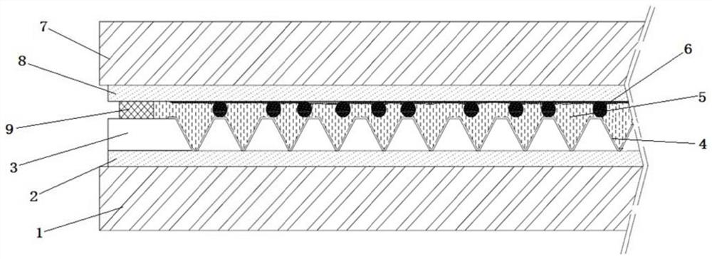
[0029] Such as figure 1 The liquid crystal photocontrol device shown, its manufacture method is as follows:
[0030] A method for manufacturing a 2D and 3D switchable liquid crystal light controller, comprising the following steps:
[0031] S1. First sputter a layer of indium tin oxide lower pattern conductive layer 2 on the lower glass substrate 1, after sputtering a layer of indium tin oxide lower pattern conductive layer 2 on the lower glass substrate 1, and then pass the yellow light process or etching paste process to oxidize The patterned conductive layer 2 under the indium tin oxide is trimmed, so that the patterned conductive layer 2 under the indium tin oxide is consistent with the shape of the lower glass substrate 1, and the patterned conductive glass under the indium tin oxide is formed after the two are bonded together;
[0032] S2. Further, continue laying a layer of zigzag microstructure pattern substrate layer 3 on the formed patterned conductive glass under t...
Embodiment 2
[0041] Such as figure 1 The shown liquid crystal photocontroller includes an upper glass substrate 7 and a lower glass substrate 1, wherein a patterned conductive layer 8 on indium tin oxide is arranged below the upper glass substrate 7, and then a patterned conductive layer 8 is placed on the upper glass substrate 7. Continue to set a layer of polyimide space ball mixture 6, the set polyimide space ball mixture 6 is made by fully mixing polyimide liquid and space balls with a diameter of 5-8um, and then on the lower glass substrate 1 A layer of indium tin oxide lower patterned conductive layer 2 that is completely consistent with indium tin oxide upper patterned conductive layer 8 is provided on it, and then a zigzag microstructure patterned substrate layer is continuously arranged on the lower indium tin oxide patterned conductive layer 2 3. A layer of polyimide alignment layer 4 is also arranged on the set microstructure pattern substrate layer 3, and finally the polyimide ...
PUM
 Abstract
Description
Claims
Application Information
