
Correction method and system for CMOS image sensor and image processing equipment

An image sensor and correction method technology, applied in the field of image processing, can solve problems such as affecting image quality, inaccurate correction results, and changes in correction parameters, and achieve the effects of improving image quality, accurate and reliable correction results, and eliminating column noise.

Pending Publication Date: 2021-05-04
HEFEI MEIYA OPTOELECTRONICS TECH
View PDF0 Cites 1 Cited by
  • Summary
  • Abstract
  • Description
  • Claims
  • Application Information

AI Technical Summary

Problems solved by technology

[0004] However, the above-mentioned method of obtaining and storing sensor calibration parameters in advance is not applicable in occasions where the temperature changes significantly, because the temperature change will affect the calibration parameters, resulting in inaccurate calibration results and affecting the quality of the image; The method of correcting parameters may change after the equipment is used for a period of time, which will also lead to inaccurate calibration results and affect the quality of the image

Method used


Image

  • Correction method and system for CMOS image sensor and image processing equipment
  • Correction method and system for CMOS image sensor and image processing equipment
  • Correction method and system for CMOS image sensor and image processing equipment

Examples


Embodiment Construction

[0041] Embodiments of the present invention are described in detail below, examples of which are shown in the drawings, wherein the same or similar reference numerals designate the same or similar elements or elements having the same or similar functions throughout. The embodiments described below by referring to the figures are exemplary only for explaining the present invention and should not be construed as limiting the present invention.

[0042] In describing the present invention, it should be understood that the terms "center", "longitudinal", "transverse", "upper", "lower", "front", "rear", "left", "right", " The orientations or positional relationships indicated by "vertical", "horizontal", "top", "bottom", "inner" and "outer" are based on the orientations or positional relationships shown in the drawings, and are only for the convenience of describing the present invention and Simplified descriptions, rather than indicating or implying that the device or element refe...


PUM


Abstract

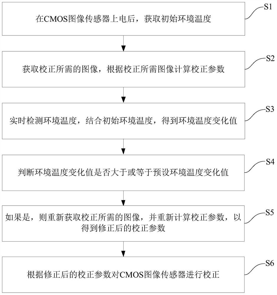
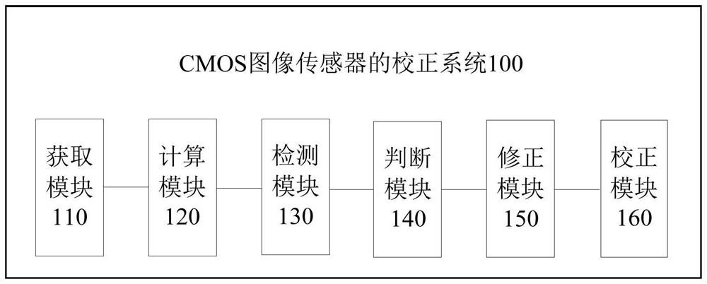
The invention provides a correction method and system for a CMOS image sensor and image processing equipment, and the method comprises the following steps: obtaining an initial environment temperature after the CMOS image sensor is powered on; acquiring an image required by correction, and calculating a correction parameter according to the image required by correction; acquiring an environment temperature change value; judging whether the environment temperature change value is greater than or equal to a preset environment temperature change value; if yes, obtaining the image needed by correction again, calculating the correction parameters again, and obtaining the corrected correction parameters; and correcting the CMOS image sensor according to the corrected correction parameters. In the working process of equipment, the correction parameters of the CMOS image sensor can be corrected according to the environment temperature change condition, the accuracy and reliability of the correction parameters are improved, the temperature adaptability of the CMOS image sensor is improved, the correction result is accurate and reliable, column noise is effectively eliminated, and the image quality is improved.

Description

technical field [0001] The invention relates to the technical field of image processing, in particular to a calibration method, system and image processing equipment of a CMOS image sensor. Background technique [0002] At present, the mainstream processing structure of CMOS (Complementary Metal Oxide Semiconductor, Complementary Metal Oxide Semiconductor) image sensor system is to use a column-sharing processing circuit, that is, each column of pixels shares a set of signal processing circuits. The most obvious problem with this structure is that the columns The column noise problem caused by the mismatch of the shared processing circuit is called column fixed pattern noise. Column fixed pattern noise can be clearly observed in uncorrected CMOS image sensors, appearing as bright and dark "vertical lines" on the image. Therefore, when in use, each column of the CMOS image sensor needs to be corrected to eliminate these "vertical lines", that is, to eliminate column fixed pa...

Claims


Application Information

Patent Timeline
Patent Type & Authority Applications(China)
IPC IPC(8): H04N5/357H04N5/365
CPCH04N25/60H04N25/67
Inventor 陈园园周楠
Owner HEFEI MEIYA OPTOELECTRONICS TECH
Learn More