Group III nitride substrate preparation method and semiconductor device
A technology of nitride and nitride layer, which is applied in the direction of semiconductor devices, electrical components, nanotechnology, etc., and can solve the problems of impurity ion residues, material defects, uneven size, etc.
- Summary
- Abstract
- Description
- Claims
- Application Information
AI Technical Summary
Problems solved by technology
Method used
Image
Examples
preparation example Construction
[0039] Based on the same inventive concept, the present invention also provides a method for preparing a III-nitride substrate, such as Figure 4 shown, including the following steps:
[0040] S1, forming 50nm porous SiO on the substrate surface 2 layer, where the SiO 2 The pores of the layer are through holes and are arranged periodically; among them, porous SiO is formed on the surface of the substrate 2 The layer is specifically: growing SiO on the surface of the substrate 2 layer, by etching method on the SiO 2 The surface of the layer forms a through-hole structure with periodic arrangement.
[0041]S2, covering the porous SiO with a 50nm porous metal mask layer 2 layer, wherein the porous metal mask layer is porous with the porous SiO 2 The pores of the layer correspond one-to-one and have the same pore size, and the lower surface of the porous metal mask layer has a plurality of nanoscale protrusion structures to match the porous SiO 2 The layer forms a hollow st...
Embodiment 1
[0047] Example 1 This example provides a method for preparing an AlN nanocolumn composite substrate
[0048] The method comprises the steps of:
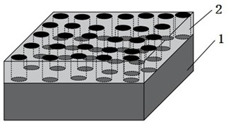
[0049] 1. Formation process of porous SiO2 layer
[0050] Such as figure 1 As shown, the process includes:
[0051] (1) Put the sapphire substrate 1 into the ion-enhanced chemical vapor deposition equipment, pass through silane and carbon dioxide gas, and form a layer of SiO with a thickness of 100nm on the sapphire surface 2 layer.
[0052] (2) will grow with SiO 2 The sapphire substrate of the layer is put into the reactive ion etching machine, and the SiO 2 Layer etched into porous SiO with periodically arranged circular vias 2 In layer 2, the hole diameter is 500nm, the depth is 100nm, and the distance between adjacent holes is 1000nm.
[0053] 2. AlN nanocolumn formation process
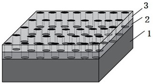
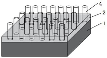
[0054] Such as figure 2 and image 3 As shown, the process includes:
[0055] (1) A Ni metal mask layer 3 with a diameter of 500nm, a pitc...
Embodiment 2
[0061] Embodiment 2 This embodiment provides a method for preparing a GaN nanopillar composite substrate, the method comprising:
[0062] (1) Put the silicon carbide substrate into the ion-enhanced chemical vapor deposition equipment, pass through silane and carbon dioxide gas, and form a layer of SiO with a thickness of 50nm on the sapphire surface 2 layer.
[0063] (2) will grow with SiO 2 The sapphire substrate of the layer is put into the reactive ion etching machine, and the SiO 2 Layer etched into porous SiO with periodically arranged circular vias 2 layer, the hole diameter is 50nm, the depth is 50nm, and the distance between adjacent holes is 600nm.
[0064] (3) A Ti metal mask layer with a diameter of 50nm and a pitch of 600nm and periodically arranged circular holes is covered on the porous SiO 2 layer surface, the thickness of the Ti metal mask layer is 50nm, and the protruding structure on the lower surface is 100nm, so that the porous SiO 2 The layer forms a ...
PUM
| Property | Measurement | Unit |
|---|---|---|
| height | aaaaa | aaaaa |
| thickness | aaaaa | aaaaa |
| diameter | aaaaa | aaaaa |
Abstract
Description
Claims
Application Information


