
Process chamber of semiconductor process equipment and semiconductor process equipment

A technology of process chamber and process equipment, applied in semiconductor/solid-state device manufacturing, metal material coating process, coating, etc., can solve problems such as pin breakage, contact state change, collision, etc.

Active Publication Date: 2021-05-18
BEIJING NAURA MICROELECTRONICS EQUIP CO LTD
View PDF6 Cites 4 Cited by
  • Summary
  • Abstract
  • Description
  • Claims
  • Application Information

AI Technical Summary

Problems solved by technology

The conical surface of the Pin cooperates with the conical surface on the base as the sealing surface to seal, but the self-weight of the Pin cannot guarantee a good seal. If the pressure difference between the front and back of the Wafer increases, the Pin may be blown up, affecting the sealing effect of the sealing surface.
If the sealing effect of the pin cone surface is not good, the chamber gas will enter between the wafer and the surface of the base, which will affect the back pressure, cause the contact state between the wafer and the base surface to change, and the temperature of the wafer to change, which will adversely affect the process results
[0004] At the same time, there is a gap between the Pin hole and the Pin of the existing CVD base. This gap ensures that the Pin slides smoothly in the hole. This gap causes a certain inclination angle between the Pin and the Pin hole of the base. There is an interaction force on the wall. After running a large number of films, this force will cause collisions and jams between the Pin and the base hole during the lifting process, which will cause problems such as wafer sliding, Pin breakage, and particles.

Method used


Image

  • Process chamber of semiconductor process equipment and semiconductor process equipment
  • Process chamber of semiconductor process equipment and semiconductor process equipment
  • Process chamber of semiconductor process equipment and semiconductor process equipment

Examples


Embodiment Construction

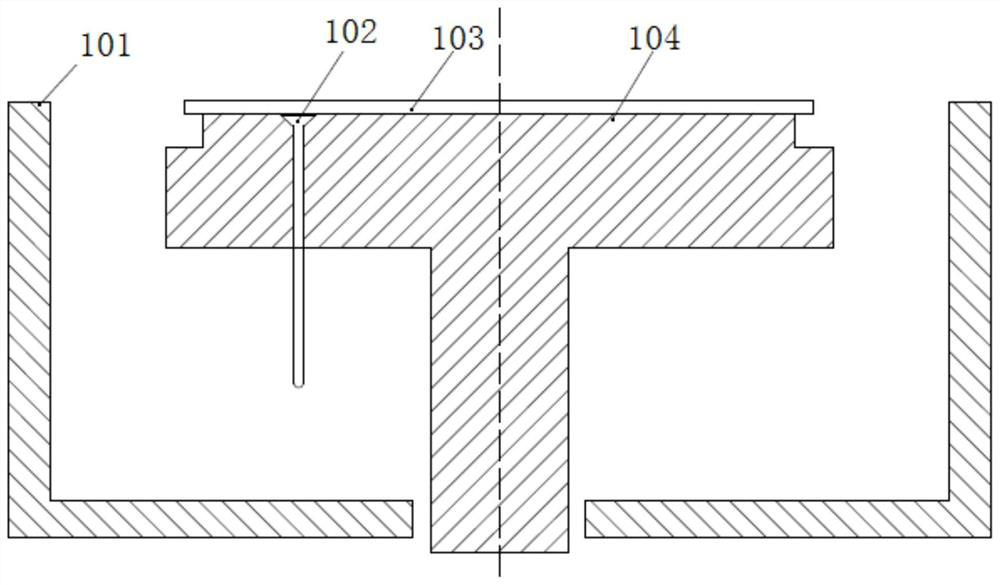
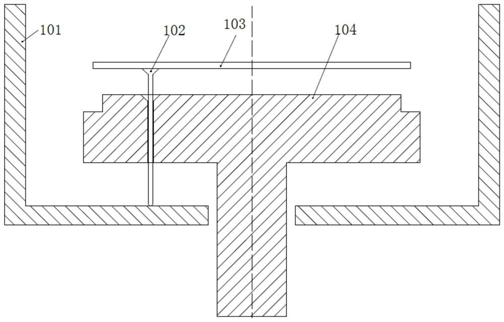
[0038] Such as figure 1 and figure 2 As shown, the existing CVD chamber includes: a chamber 101 , support pins 102 , a wafer 103 , and a base 104 . The height of the base 104 is adjusted by the lifting mechanism to realize switching between the transmission position and the process position. In the existing structure, the support needle is sealed by its own weight at the tapered surface, and there is a gap between the pinhole on the base and the support needle 102. This gap ensures that the support needle 102 slides smoothly in the hole and guides it. There is a certain inclination angle between the needle 102 and the pinhole of the base, and there is an interaction force between the support pin 102 and the side wall of the pinhole of the base. There are collisions and jams between the holes, which will cause problems such as slippage of the wafer 103, breakage of the support pins 102, and particles. The structure of the base 104 has the following problems:

[0039] 1. Th...


PUM


Abstract

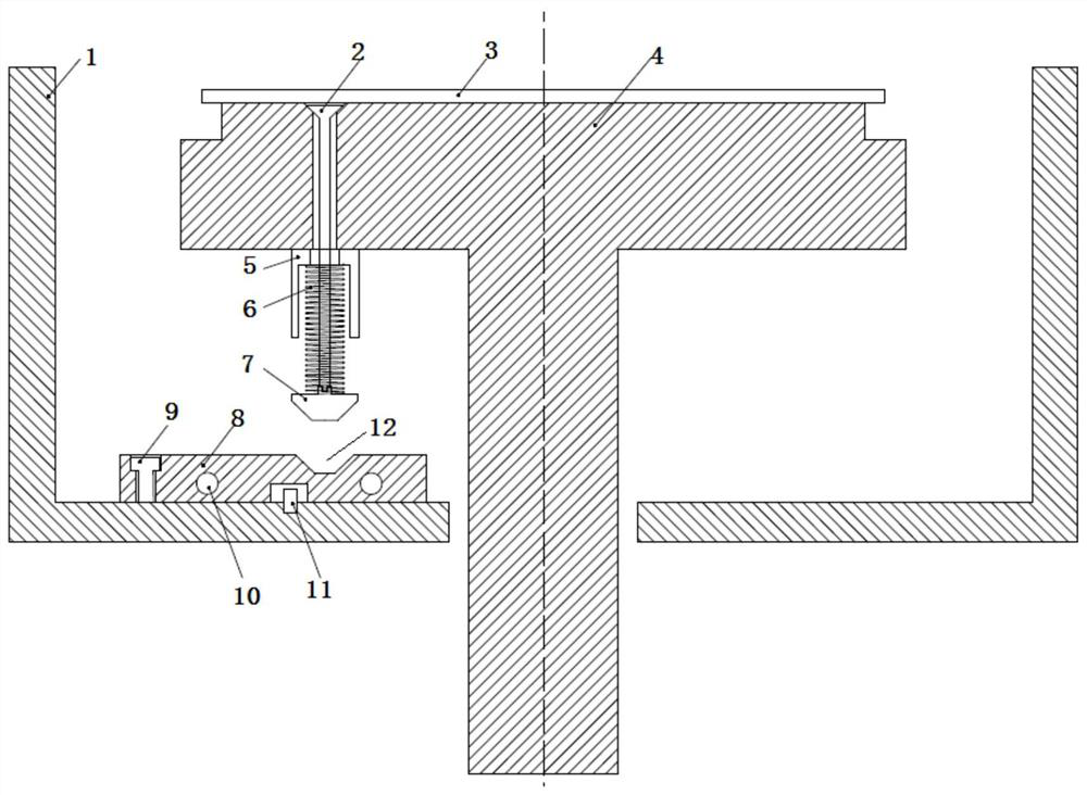
The invention discloses a process chamber of semiconductor process equipment and the semiconductor process equipment. A liftable base is arranged in the process chamber, and a plurality of support pins are arranged in the base. A plurality of needle holes penetrating through the upper and lower surfaces of the base are formed in the base, sealing grooves are formed in the top ends of the needle holes, and baffle rings in one-to-one correspondence with the needle holes are arranged on the lower surface of the base. Sealing heads are arranged at the top ends of the support pins, the sealing heads are matched with the sealing grooves in shape, positioning blocks are arranged at the bottom ends of the support pins, elastic pieces in a compressed state are arranged between the positioning blocks and the baffle rings in a sleeving mode, and when the base ascends to a process position, the sealing heads are matched with the sealing grooves in a sealing mode. A positioning plate is arranged on the bottom wall of the process chamber, a first positioning part matched with the positioning blocks in shape is arranged on the upper surface of the positioning plate, when the base descends to a transmission position, the positioning blocks are in positioning fit with the first positioning part, and the support pins extend out of the upper surface of the base. Air leakage at the sealing heads of the support pins and the sealing grooves of the needle holes can be reduced, and the process effect is improved.

Description

technical field [0001] The present invention relates to the field of semiconductor equipment, and more specifically, to a process chamber of semiconductor process equipment and semiconductor process equipment. Background technique [0002] In recent years, semiconductor equipment has developed rapidly, involving semiconductors, integrated circuits, solar panels, flat-panel displays, microelectronics, light-emitting diodes, etc., and these devices are mainly composed of several layers of thin films with different material thicknesses formed on wafers . Taking a CVD chamber as an example, Wafer is delivered to the chamber before film formation, and Wafer is taken out after film formation is completed. During this process, the Pin (support pin) lifts the Wafer, so that there is a certain distance between the Wafer and the base, ensuring that the robot can have space to enter the lower surface of the Wafer and take the Wafer away. In order to ensure the film quality of the pro...

Claims


Application Information

Patent Timeline
Patent Type & Authority Applications(China)
IPC IPC(8): C23C16/458H01L21/687
CPCC23C16/4585H01L21/68742
Inventor 田西强
Owner BEIJING NAURA MICROELECTRONICS EQUIP CO LTD
Learn More