Semiconductor chip and manufacturing method thereof

A manufacturing method and semiconductor technology, applied in the direction of semiconductor/solid-state device manufacturing, semiconductor devices, semiconductor/solid-state device components, etc., can solve the problems of difficult process, small effective window, yield loss, etc. The effect of reducing difficulty and improving yield rate

Inactive Publication Date: 2021-05-25
YANGTZE MEMORY TECH CO LTD
View PDF2 Cites 0 Cited by
  • Summary
  • Abstract
  • Description
  • Claims
  • Application Information

AI Technical Summary

Problems solved by technology

In the existing scribing method, the effective window of the process is small and the process is difficult. The speed of the moving scribing knife and the rotational speed of the scribing knife must be strictly controlled to reduce chipping on the chip during scribing.
In addition, the minimum cutting width of a general dicing blade is about 40 μm, and the width of the scribe lane is 75 μm. During cutting, the passivation layer and polyimide layer will be squeezed to both sides, and even the chip will be damaged, resulting in a loss of yield.

Method used


Image

  • Semiconductor chip and manufacturing method thereof
  • Semiconductor chip and manufacturing method thereof
  • Semiconductor chip and manufacturing method thereof

Examples


Embodiment Construction

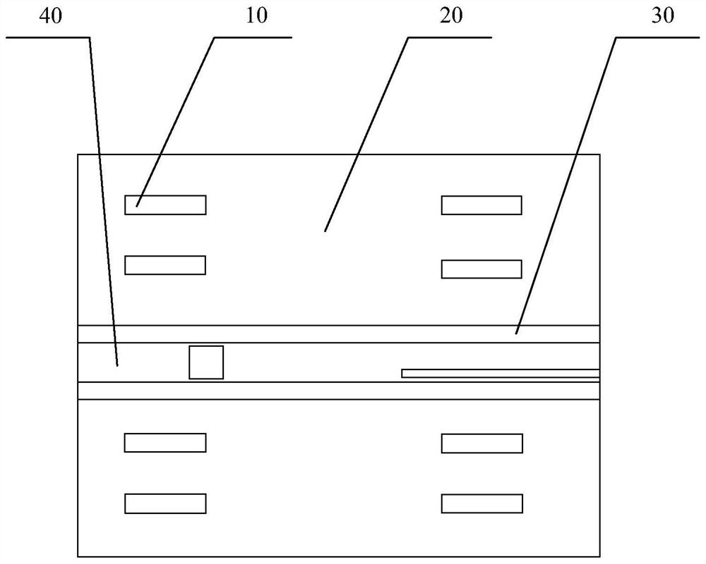
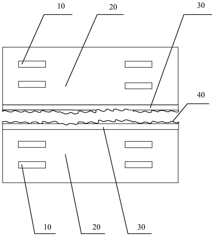
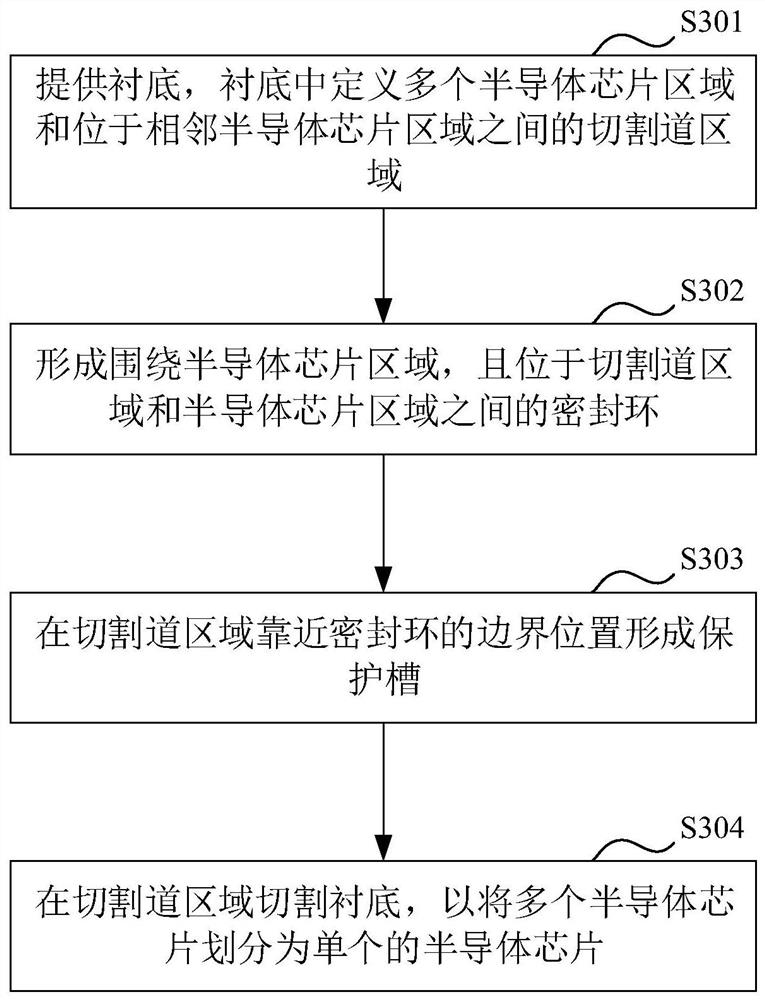
[0038]Various embodiments of the present invention will be described in more detail below with reference to the accompanying drawings. In each of the drawings, the same elements are expressed by the same or similar reference numerals. For the sake of clarity, the various parts in the drawings are not drawn. In addition, some well-known portions may not be shown in the figure.

[0039]DETAILED DESCRIPTION OF THE PREFERRED EMBODIMENTS Many of the specific details of the present invention are described below, such as structural, material, size, processing processes, and techniques of the components, in order to understand the present invention more clearly. However, as will be apparent to those skilled in the art, the present invention may be implemented without follow these specific details.

[0040]It should be understood that when the structure of the component is described, when a layer, one area is called the other layer, another region "upper" or "above", it may refer to directly locat...


PUM

PropertyMeasurementUnit
widthaaaaaaaaaa

Abstract

The invention discloses a semiconductor chip and a manufacturing method thereof. The manufacturing method of the semiconductor chip comprises the following steps: providing a substrate, wherein a plurality of semiconductor chip areas and cutting channel areas between adjacent semiconductor chip areas are defined in the substrate; forming a sealing ring surrounding the semiconductor chip region and located between the scribe line region and the semiconductor chip region; forming a protection groove in the boundary position, close to the sealing ring, of the semiconductor chip cutting channel area; and cutting the substrate in the scribe line region to divide the plurality of semiconductor chips into individual semiconductor chips. According to the semiconductor chip manufacturing method, the difficulty of a scribing process can be reduced, and the yield of chips can be improved.

Description

Technical field[0001]The present invention relates to the field of semiconductor devices, and in particular, to a semiconductor chip and a method of fabricating thereof.Background technique[0002]In the existing new 3D NAND product architecture, the storage unit area (Cell) and the peripheral (CMOS) are fabricated on different wafers, and the circuit is connected together by three-dimensional special processes, from the back cover Cell, the wafer, The circuit is then protected by a passivation film and a polyimide layer (PASSIVATION FILM) and a polyimide layer according to the package requirements.[0003]Before the use of the electronic product, the die (DIE) needs to be separated (drawn), and due to the passivation layer extremely easy to fall off, even damaged the duck, it is extremely high requirements for the drawing process. In an existing diaphragm method, the effective window of the process is small, the process is difficult, and the speed of moving the scribe cutting knife and...

Claims


Application Information

Patent Timeline
Patent Type & Authority Applications(China)
IPC IPC(8): H01L23/31H01L25/16H01L21/78H01L27/11517H01L27/11563
CPCH01L23/3121H01L25/162H01L21/78H10B41/41H10B43/35
Inventor 宋林王永庆陈赫伍术
Owner YANGTZE MEMORY TECH CO LTD
Why Eureka
Try Eureka