Touch control chip simulation pressing test jig

A technology for testing jigs and touch chips, applied in electronic circuit testing, measuring electricity, measuring devices, etc., can solve the problems of chip damage, waste of time, low test efficiency, etc., and achieve the effect of improving efficiency

Inactive Publication Date: 2021-06-01
张雪
View PDF0 Cites 3 Cited by
  • Summary
  • Abstract
  • Description
  • Claims
  • Application Information

AI Technical Summary

Problems solved by technology

[0004] The purpose of the present invention is to provide a touch chip simulation press test fixture to solve the problem that the existing touch chips are tested one by one when testing, the test efficiency is low, and it is a waste of time, and when testing, It is prone to the problem that the probe exerts too much pressure on the chip, resulting in damage to the chip

Method used


Image

  • Touch control chip simulation pressing test jig
  • Touch control chip simulation pressing test jig
  • Touch control chip simulation pressing test jig

Examples


Embodiment Construction

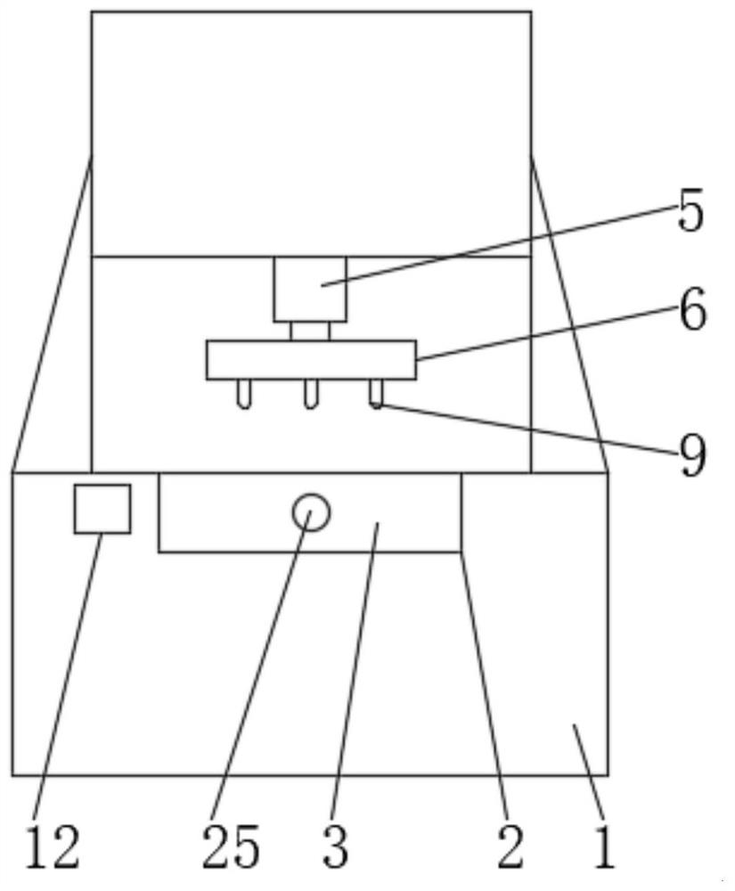
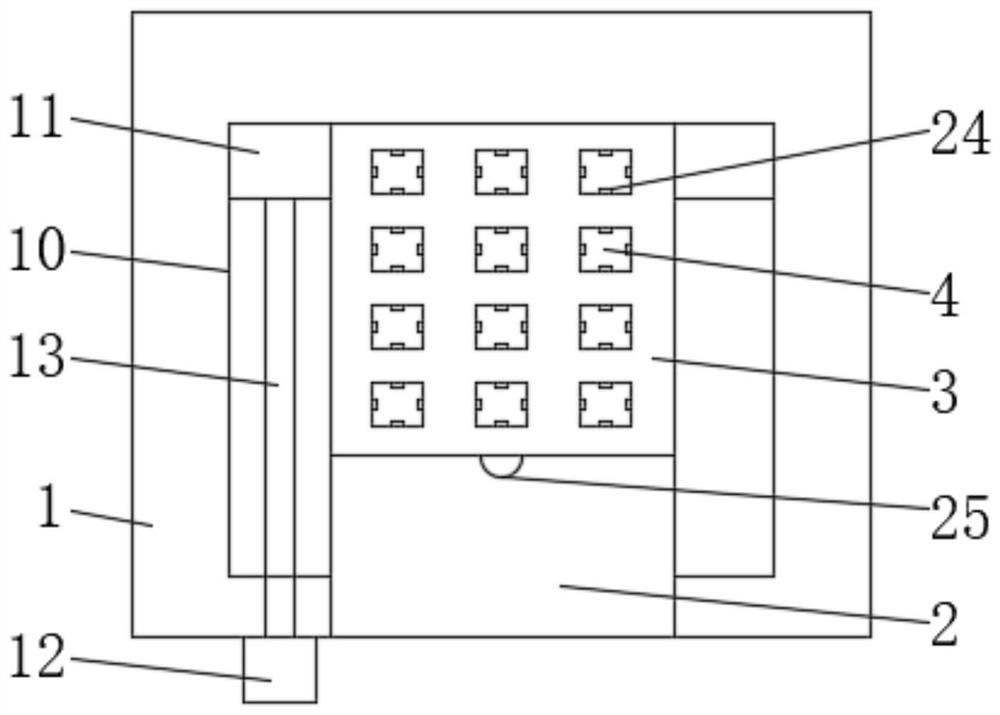
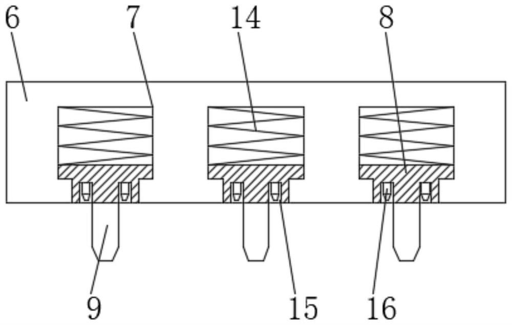
[0021] see figure 1 , figure 2 , image 3 , touch chip simulation press test fixture, including test machine body 1, a chute 2 is provided on the machine table of the test machine body 1, a plate 3 is set inside the chute 2, and a chip groove 4 is provided on the plate 3 , the testing machine body 1 is equipped with a cylinder 5 through screws, and the lower end of the cylinder 5 is equipped with a lifting plate 6 through screws. The probe 9 is mounted by screws.

[0022] see figure 1 , figure 2 , the number of chip slots 4 and probes 9 is equal, and the positions correspond to each other, the chip slots 4 and probes 9 are evenly distributed on the plate 3 and the lifting plate 6 respectively, by controlling multiple probes 9 to multiple chip slots 4 The internal chip is tested, which can improve the efficiency of the test.

[0023] see figure 2 , both sides of the inner wall of the chute 2 are provided with limit slides 10, and both sides of the plate 3 are installe...


PUM


Abstract

The invention discloses a touch control chip simulation pressing test jig which comprises a test machine body. A sliding groove is formed in a machine table of the test machine body, a chip groove is formed in a plate, a buffer groove is formed in a lifting plate, a lifting block is arranged in the buffer groove in a sleeved mode, and a probe is installed on the lifting block. The chip can be conveniently put in or taken out by controlling the plate to move out of or move into the sliding groove; by controlling the magnetism of the electromagnet, the pressing rod can be controlled to be retracted into the cavity or moved out of the cavity, so that one end of the pressing rod can be conveniently controlled to press the chip, the chip is fixed in the chip groove, and the situation that the test is influenced by movement and dislocation of the chip is avoided; the laser lamp emits light rays along the probe to irradiate the chip, so that the probe and the chip can be positioned, and the condition that the probe and the chip are staggered is avoided; the plurality of probes are controlled to test the chips in the plurality of chip grooves, so that the test efficiency can be improved; and the first spring is used for buffering, so that the condition that the chip is crushed can be avoided.

Description

technical field [0001] The invention belongs to the technical field of touch chips, in particular to a touch chip simulation pressing test jig. Background technique [0002] Touch chip refers specifically to single-point or multi-point touch technology, and its application range is mobile phones, computers, etc. "Touch" here specifically refers to single-point or multi-touch technology; chip is IC, which refers to a metal sheet or non-metal sheet whose end surface can be integrated with friction lining and friction material layer, and generally refers to all electronic devices. A component is a circuit module that integrates a variety of electronic components on a silicon board to achieve a specific function. It is the most important part of electronic equipment, undertaking the functions of computing and storage. The application range of integrated circuits covers almost all electronic equipment for military and civilian use. A small silicon chip containing integrated ci...

Claims


Application Information

Patent Timeline
Patent Type & Authority Applications(China)
IPC IPC(8): G01R31/28
CPCG01R31/2825G01R31/2887G01R31/2891
Inventor 张雪
Owner 张雪
Why Eureka
Try Eureka