Communication system and method

A technology of communication system and clock signal, which is applied in the field of communication system to achieve the effect of saving the number of pins

Pending Publication Date: 2021-06-01
GUANGDONG TOPSTAR TECH
View PDF0 Cites 1 Cited by
  • Summary
  • Abstract
  • Description
  • Claims
  • Application Information

AI Technical Summary

Problems solved by technology

When the master device communicates with each slave device, it takes time to chip-select each slave device, and it needs to wait for the transmission to complete before sending the next frame of data, so high-speed communication between multiple slave devices cannot be performed

Method used


Image

  • Communication system and method
  • Communication system and method
  • Communication system and method

Examples


Embodiment 1

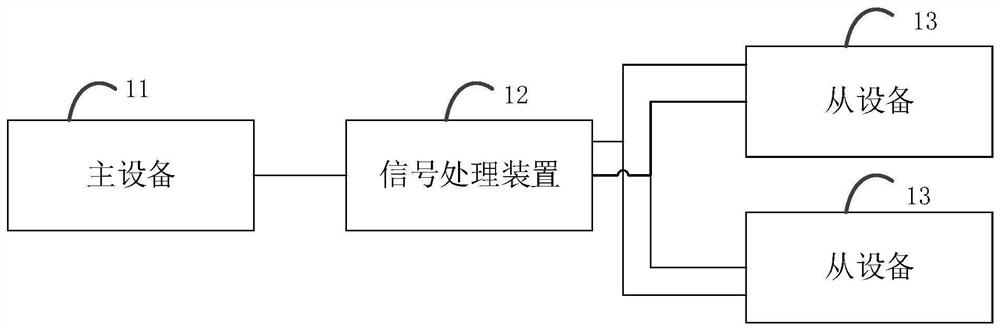
[0046] figure 2 It is a schematic structural diagram of a communication system provided by Embodiment 1 of the present invention. This embodiment is applicable to the communication between a master device and a slave device. The system includes: a master device 11, a signal processing device 12, and at least one slave device 13;

[0047] The master device 11 is configured to generate a data signal with a set format when the data sending condition is satisfied, and send it to the signal processing device 12 through the data output pin;

[0048] The signal processing device 12 is used to generate an integer clock signal according to the data signal, and send the data signal to each slave device 13 through the data output pin, and send the integer clock signal to each slave device 13 through the count pin;

[0049] Each slave device 13 is used to receive the data signal according to the integer clock signal;

[0050] Wherein, the data signal includes: at least one byte length i...

Embodiment 2

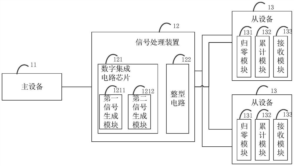
[0062] image 3 It is a schematic structural diagram of a communication system provided by Embodiment 2 of the present invention. The technical solution of this embodiment is further optimized on the basis of the above-mentioned technical solution, such as image 3 As shown, the embodiment of the present invention further optimizes the signal processing device 12, which specifically includes a digital integrated circuit chip 121 and an integer circuit 122; wherein, the digital integrated circuit chip 121 is used to generate a digital clock signal according to a data signal, and convert the digital clock signal to The clock signal is sent to the integer circuit through the clock pin, and the data signal is sent to each slave device through the data output pin; the integer circuit 122 is used to convert the digital clock signal into an integer clock signal and convert the integer clock The signal is sent to each slave device 13 via the count pin.

[0063] In this embodiment, t...

Embodiment 3

[0113] Image 6 It is a flow chart of a communication method provided by Embodiment 3 of the present invention. The method is executed by the communication system provided by any embodiment of the present invention, and includes the following steps:

[0114] S310. When the data sending condition is met, the master device generates a data signal with a set format, and sends it to the signal processing device through a data output pin.

[0115] S320. The signal processing device generates an integer clock signal according to the data signal, and sends the data signal to at least one slave device through a data output pin, and sends the integer clock signal to each slave device through a count pin described slave device.

[0116] S330. Each of the slave devices receives the data signal according to the integer clock signal.

[0117] Wherein, the data signal includes: at least one byte length information and byte data information corresponding to each byte length information, and ...


PUM


Abstract

The embodiment of the invention discloses a communication system and method. The system comprises a master device, a signal processing device and at least one slave device. The main devicet is used for generating a data signal in a set format when a data sending condition is met, and sending the data signal to the signal processing device through a data output pin; the signal processing device is used for generating an integer clock signal according to the data signal, sending the data signal to each slave device through the data output pin, and sending the integer clock signal to each slave device through the counting pin; each slave device is used for receiving the data signal according to the integer clock signal, wherein the data signal comprises at least one piece of byte length information and byte data information corresponding to each piece of byte length information, and the quantity of the byte length information is determined by the quantity of the slave devices, so that the problem that chip selection signals must be sent to the slave devices in the communication process of the master device and the slave devices in the prior art is solved; the effect of high-speed communication between the master device and the slave device is achieved.

Description

technical field [0001] Embodiments of the present invention relate to communication technologies, and in particular, to a communication system and method. Background technique [0002] With the development of communication technology, chips are more and more widely used in production and life, and chips can communicate in a way of serial peripheral interface (Serial Peripheral Interface, SPI). SPI is a full-duplex four-wire synchronous serial peripheral interface first proposed by Motorola. It adopts a master-slave mode architecture and supports single-master and multi-slave mode applications. [0003] figure 1 A connection schematic diagram of a master device and a slave device in the prior art is provided. like figure 1 As shown, the MOSI line is used for master device data output and slave device data input; MISO line is used for master device data input and slave device data output; CLK line is used to transmit the clock signal generated by the master device; CS1 line...

Claims


Application Information

Patent Timeline
IPC IPC(8): G06F13/42G06F15/78G06F1/12
CPCG06F13/4291G06F15/7807G06F1/12
Inventor 黄勇王志成王亚平唐海元伍芬智张钊徐必业吴丰礼
Owner GUANGDONG TOPSTAR TECH
Why Eureka
Try Eureka