
Repair method of DRAM (Dynamic Random Access Memory) storage array and related equipment

A storage array and repair method technology, applied in the field of chips, can solve problems such as yield loss and unrepairable chips, and achieve the effect of improving yield and solving low yield

Active Publication Date: 2021-06-04
XI AN UNIIC SEMICON CO LTD
View PDF3 Cites 1 Cited by
  • Summary
  • Abstract
  • Description
  • Claims
  • Application Information

AI Technical Summary

Problems solved by technology

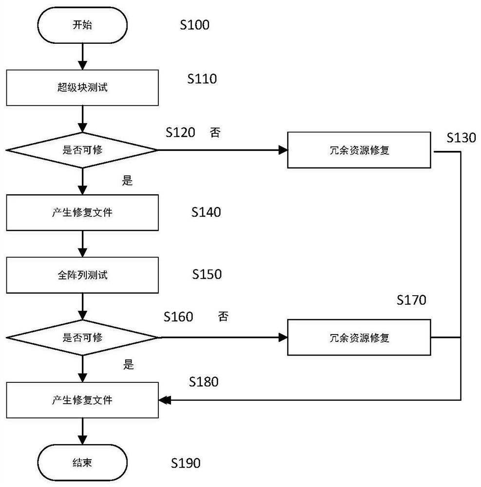
However, in practical applications, when the existing repair method is repairing, in some cases, when there is a super block that can be repaired but the remaining redundant resources do not satisfy other failed sub-blocks, the current repair method will use these only Chips that meet the repair requirements of the failed super block are determined to be unrepairable chips, but in fact, in many cases, chips that can be completely repaired by the failed super block can also be used as normal chips, which leads to the fact that the existing conventional repair methods will be practically impossible. It can meet the situation of the unrepairable chip determined by the chip actually used, resulting in the loss of yield rate

Method used


Image

  • Repair method of DRAM (Dynamic Random Access Memory) storage array and related equipment
  • Repair method of DRAM (Dynamic Random Access Memory) storage array and related equipment
  • Repair method of DRAM (Dynamic Random Access Memory) storage array and related equipment

Examples


Embodiment Construction

[0101] The present invention will be described in further detail below in conjunction with the accompanying drawings and embodiments, so that those skilled in the art can implement it with reference to the description.

[0102]It should be understood that terms such as "having", "comprising" and "including" used herein do not exclude the presence or addition of one or more other elements or combinations thereof.

[0103] In addition, it should be noted that, unless otherwise specified and limited, the terms "setting" and "connection" should be understood in a broad sense. For example, it may be a fixed connection or a detachable connection; it may be a direct connection or an indirect connection through an intermediary; it may be an integral connection or an internal communication between two components. Signal transmission and data communication can also be performed between two components. Those of ordinary skill in the art can understand the specific meanings of the above ...


PUM


Abstract

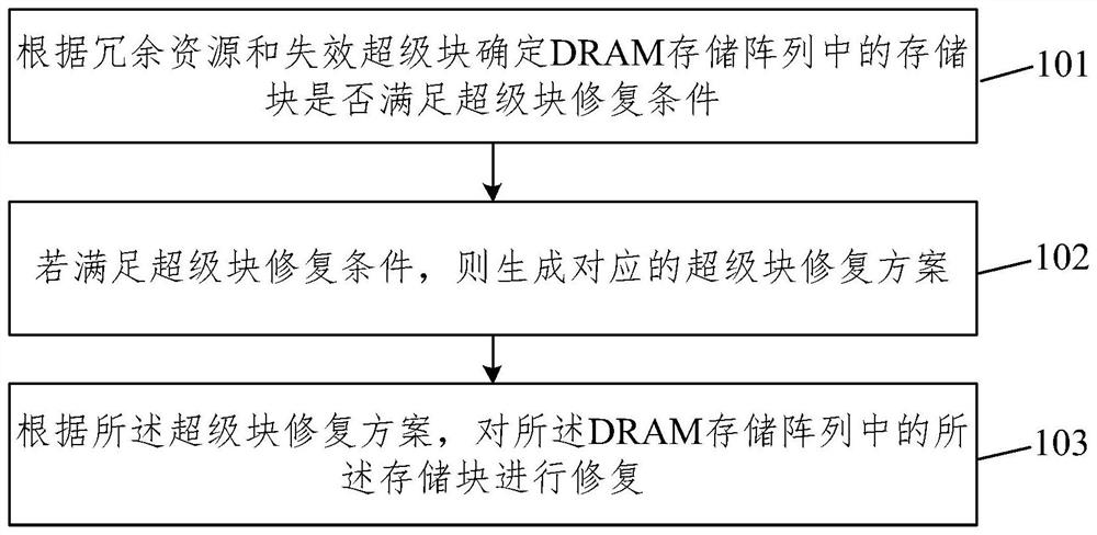
The embodiment of the invention provides a method for repairing a DRAM (Dynamic Random Access Memory) storage array and related equipment. The method and the equipment are used for solving the problem of yield loss in a conventional repairing process. The method comprises the steps that according to redundant resources and invalid super blocks, whether the storage blocks in the DRAM storage array meet super block repairing conditions or not is determined, the super block repairing conditions are used for judging whether the number of the redundant resources in the DRAM storage array meets the repairing number of the invalid super blocks of the storage blocks or not, and if yes, the redundant resources in the DRAM storage array meet the repairing number of the invalid super blocks of the storage blocks; the redundant resource and the failed super block belong to the storage block, the redundant resource is a storage medium used for repairing the failure in the storage block, the storage block comprises a super block and a sub-block, and the failed super block is a super block which is detected to be failed in the storage block; if the super block repairing condition is met, generating a corresponding super block repairing scheme; and according to the super block repairing scheme, repairing the storage block in the DRAM storage array.

Description

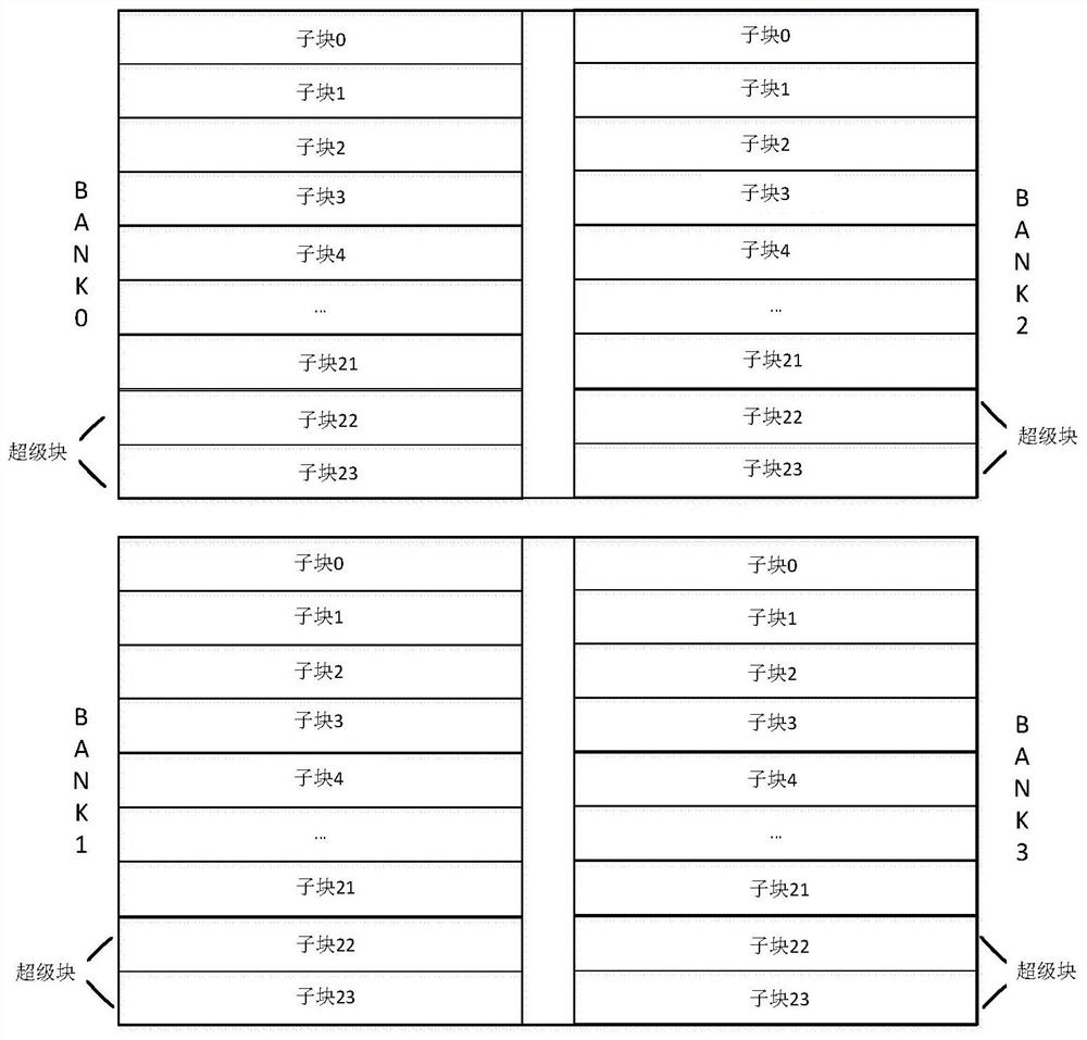
technical field [0001] Embodiments of the present invention relate to the field of chip technology, and in particular, relate to a method for repairing a DRAM storage array and related equipment. Background technique [0002] In the chip, the DRAM storage array (Dynamic random access memory, DRAM for short) often assumes the role of secondary cache and temporary storage. In the normal use process, sometimes the DRAM storage array is used The storage medium corresponding to some addresses in the storage block is used as a first-level cache, or this part of addresses is used for internal logic detection. Therefore, it is required that the reliability level of the storage medium corresponding to this part of the address is higher, and this part of the logical address also needs to be repaired first in the repair process, so it is often called the super block in the storage block of the DRAM array, and in the storage In the block, the sub-blocks other than the super block are o...

Claims


Application Information

Patent Timeline
Patent Type & Authority Applications(China)
IPC IPC(8): G11C29/00
CPCG11C29/72G11C29/883
Inventor 张朝锋王春娟王砚
Owner XI AN UNIIC SEMICON CO LTD
Learn More