
Patsnap Eureka
For R&D, Patsnap Eureka makes reading and utilizing patents & technical documents easy.
Patsnap Eureka AIR
Designed for self-driven R&D workflows. Generate viable solutions, solve complex R&D challenges, empower your innovation with AI.

Patsnap Eureka Materials
Designed for material experts only. Revolutionize your material R&D, from search, analyze, to developing new materials.

TechResearch
Generate reliable direction feasibility study reports for your R&D in just a few steps.

TechSeek
Discover and master advanced knowledge NOW. Basics, ideas, possibilities, all at once.

TechMind
As an expert in R&D Theories, TechMind can generates customized viable solutions instantly.

TechRisk
Analyze your overall solution with one click, know your potential R&D risks in advance.

TechMonitor
Get weekly tech updates, stay abreast of the latest tech innovations and key insights.
BPSG film layer processing method and semiconductor intermediate product
A processing method and film layer technology, applied in semiconductor/solid-state device manufacturing, electrical components, circuits, etc., can solve problems such as deviation and affect product quality, and achieve the effect of quality assurance
- Summary
- Abstract
- Description
- Claims
- Application Information
AI Technical Summary
Problems solved by technology
Method used
Image


Examples
Embodiment 1
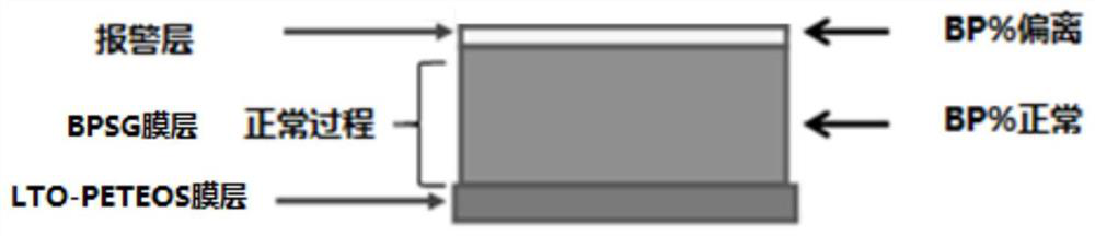
[0030] The BPSG process usually grows a layer of 2000A (Am, 1A=10A) on the wafer. -10 m) about LTO-PETEOS film layer, and then grow BPSG film layer on it, under normal circumstances, the resulting products produced after the completion of the BPSG process are as follows figure 1 shown. When the BPSG process is interrupted due to rule parameter changes or machine alarms, the resulting products at this time are as follows: figure 2 As shown, the film quality of the BPSG film layer grown during and at the end of the process interruption (ie figure 2 The film quality of the film layer grown during the normal process will be very different, especially the content of BP% will be very different. At this time if in figure 2 On the basis of the target thickness, directly rework and grow the BPSG film layer with the remaining thickness, which will cause a layer of alarm layer with different BP% concentration and different film quality in the middle of the BPSG film layer, and the ...
Embodiment 2
[0045] This embodiment is further improved on the basis of Embodiment 1. Such as Figure 5 Shown, this BPSG membrane treatment method comprises the steps:
[0046] S201. Measure the thickness of the BPSG film layer in the resulting product after the interruption of the BPSG process, and calculate the time required for dry etching and etching of the BPSG film layer; calculate the time required for dry etching and etching of the LTO-PETEOS film layer through the first thickness required time.
[0047] Such as Figure 6 As shown, the BPSG process usually grows a layer of LTO-PETEOS film layer of about 2000A on the wafer, and then grows the BPSG film layer on it (the wafer is omitted in the figure). The dry method of these two film layers The etching rate is different. The dry etching rate of the LTO-PETEOS film layer is 3300A / min (A / min), and the dry etching rate of the BPSG film layer is 6000A / min.
[0048] Before carrying out dry etching, measure the thickness of the BPSG f...
PUM
 Abstract
Description
Claims
Application Information
 - R&D Engineer
- R&D Manager
- IP Professional
- Industry Leading Data Capabilities
- Powerful AI technology
- Patent DNA Extraction
Browse by: Latest US Patents, China's latest patents, Technical Efficacy Thesaurus, Application Domain, Technology Topic, Popular Technical Reports.
© 2024 PatSnap. All rights reserved.Legal|Privacy policy|Modern Slavery Act Transparency Statement|Sitemap|About US| Contact US: help@patsnap.com