Wafer deplating process method

A process method and chip technology, which is applied in the direction of electrical components, semiconductor/solid-state device manufacturing, circuits, etc., can solve problems such as missing teeth and defective products, and achieve the effects of reducing defect rate, improving deplating effect, and improving deplating efficiency

Pending Publication Date: 2021-06-08
LENS TECH CHANGSHA
View PDF0 Cites 0 Cited by
  • Summary
  • Abstract
  • Description
  • Claims
  • Application Information

AI Technical Summary

Problems solved by technology

[0006] However, since the deplating agent is a strong acid and strong alkali with strong corrosiveness, while stripping the exposed anti-reflective coating, after a certain soaking time, the stripping agent will also start to bite the protective oil, and then the protective oil will be removed. The anti-reflection film of the covered shielding area is peeled off, forming defective products with missing teeth or over-regression defective products on the edge of protective oil.

Method used


Image

  • Wafer deplating process method
  • Wafer deplating process method
  • Wafer deplating process method

Examples


Embodiment Construction

[0042] The following will clearly and completely describe the technical solutions in the embodiments of the present invention with reference to the accompanying drawings in the embodiments of the present invention. Obviously, the described embodiments are only some, not all, embodiments of the present invention. Based on the embodiments of the present invention, all other embodiments obtained by persons of ordinary skill in the art without making creative efforts belong to the protection scope of the present invention.

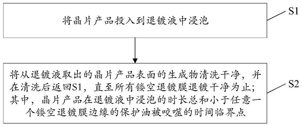
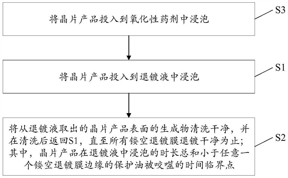
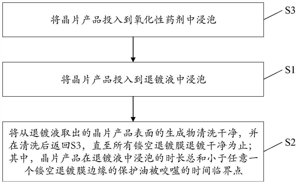
[0043] The core of the invention is to provide a wafer deplating process method to reduce the defective rate of the wafer deplating process.

[0044] Please refer to Figure 1-Figure 3 , figure 1 The flow chart of the wafer deplating process method provided for the specific embodiment of the present invention; figure 2 The flowchart of the wafer deplating process method provided by the second embodiment of the present invention; image 3 It is a flow chart...


PUM

PropertyMeasurementUnit
thicknessaaaaaaaaaa

Abstract

The invention discloses a wafer deplating process method. The wafer deplating process method comprises the steps of: putting a wafer product into a deplating solution to be soaked; and cleaning a product on the surface of the wafer product taken out from the deplating solution, and returning to the step of putting the wafer product into the deplating solution for soaking after cleaning until all the hollowed-out deplating films are deplated, wherein the sum of the soaking time of the wafer product in the deplating solution is smaller than the time critical point of biting of the protective oil at the edge of any hollow deplating film. According to the wafer deplating process method, the product on the surface of the wafer product taken out from the deplating solution is cleaned up, then the wafer product is put into the deplating solution to be soaked, the phenomenon that the product covers an antireflection film and affects the contact reaction of the antireflection film and the deplating solution is avoided, and through repeated deplating and cleaning, the deplating efficiency is improved, and the overall deplating time is shortened. Therefore, after all the hollowed-out antireflection films are completely removed, the overall deplating time does not reach the time critical point at which the protective oil on the edge of any hollowed-out antireflection film is bitten, and the reject ratio is reduced.

Description

technical field [0001] The invention relates to the technical field of deplating process in the optical glass manufacturing process, and more specifically relates to a wafer deplating process method. Background technique [0002] Chips, such as glass, ceramic and sapphire, are used in a wide range of technologies such as mobile phones, watches, and cameras. [0003] For some optical chip products, there are usually various patterns and / or characters, etc., in order to meet customers' needs for fashion, beauty and personalized appearance. [0004] During the manufacturing process of these optical wafer products, the front area of ​​the wafer is usually coated with an anti-reflection film, and then the screen pattern is printed on the anti-reflection film by printing protective oil multiple times to obtain the required anti-reflection film. The position of the film is covered and protected with protective oil, so that the anti-reflection film at the position where the protect...

Claims


Application Information

Patent Timeline
Patent Type & Authority Applications(China)
IPC IPC(8): H01L21/02
CPCH01L21/0206
Inventor 周群飞钟耀辉钟方权
Owner LENS TECH CHANGSHA
Why Eureka
Try Eureka