Supercharge Your Innovation With Domain-Expert AI Agents!

A hybrid integrated optical communication band on-chip quantum entanglement source

A hybrid integration and quantum entanglement technology, applied in optics, nonlinear optics, instruments, etc., can solve the problems of reducing the brightness of entangled two-photon, reducing the purity of entangled two-photon, and the impact of entangled two-photon application, achieving high integration, reducing The effect of using space and wide application prospects

Active Publication Date: 2022-01-07
UNIV OF ELECTRONICS SCI & TECH OF CHINA
View PDF6 Cites 0 Cited by
  • Summary
  • Abstract
  • Description
  • Claims
  • Application Information

AI Technical Summary

Problems solved by technology

In order to improve the scalability of the quantum communication system, it is necessary to increase the integration of the quantum entanglement source. Since the second-order nonlinear waveguide has the characteristics of small size and easy integration, fiber coupling is usually used to make the pump light into the second-order nonlinear waveguide. The waveguide generates entangled two-photons in the optical communication band. However, the photons generated by the spontaneous Raman scattering process of the pump light in the fiber will enter the second-order nonlinear waveguide along with the pump light, and the remaining pump light will also follow the entangled double photons. Photons are output from the second-order nonlinear waveguide and enter the entangled two-photon transmission channel. Noise photons are generated through the spontaneous Raman scattering process in the transmission fiber, thereby reducing the purity of the entangled two-photon and seriously affecting the application of the entangled two-photon.
In order to reduce the number of noise photons, the power of the pump light can be reduced, but the brightness of the entangled two-photons is inevitably reduced

Method used


Image

  • A hybrid integrated optical communication band on-chip quantum entanglement source
  • A hybrid integrated optical communication band on-chip quantum entanglement source
  • A hybrid integrated optical communication band on-chip quantum entanglement source

Examples


Embodiment Construction

[0039] The principles and features of the present invention are described below in conjunction with the accompanying drawings, and the examples given are only used to explain the present invention, and are not intended to limit the scope of the present invention.

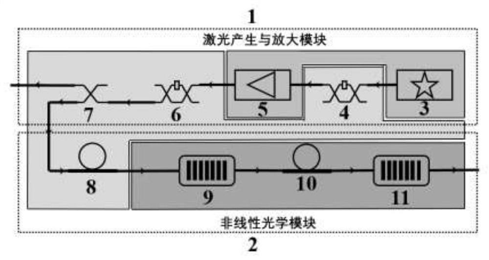
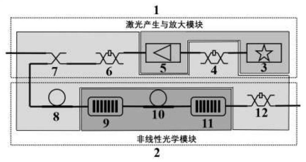
[0040] Such as figure 1 As shown, a hybrid integrated optical communication band on-chip quantum entanglement source provided by the first embodiment of the present invention includes a laser generation and amplification module 1 and a nonlinear optical module 2, the laser generation and amplification module 1 and the non-linear optical module 2 The linear optical module 2 is integrated on the same substrate material;

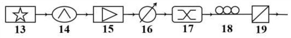
[0041] The laser generating and amplifying module 1 includes a sequentially connected continuous laser 3, an intensity modulator 4, an optical amplifier 5, an adjustable optical attenuator 6 and a beam splitter 7;

[0042] The DC pump light in the optical communication band generated by the continuo...


PUM


Abstract

The invention relates to a hybrid integrated optical communication band on-chip quantum entanglement source, including a laser generation and amplification module and a nonlinear optical module. The nonlinear optical module is formed by connecting two sections of nonlinear waveguides through a second harmonic filter. Under the action of pump light in the optical communication band, the second harmonic generation and the spontaneous parametric down-conversion process occur successively in the two nonlinear waveguides, thereby realizing the generation of quantum entangled two-photons. The second harmonic filter connecting the two waveguides can effectively suppress the remaining pump light and avoid the noise introduced by the spontaneous Raman scattering process in the entangled two-photon. All the devices required by the on-chip quantum entanglement source are integrated on the same substrate material, effectively reducing the volume of the quantum entanglement source. The hybrid integrated optical communication band on-chip quantum entanglement source proposed by the present invention has the characteristics of high integration, high brightness and low noise at the same time, and can be realized through advanced micro-nano processing and packaging technology, which is conducive to the integration and practicalization of quantum light sources develop.

Description

technical field [0001] The invention belongs to the technical field of quantum detection and quantum network, and in particular relates to a mixed and integrated on-chip quantum entanglement source in the optical communication band. Background technique [0002] Entangled two-photons in the optical communication band are the most important resources in the field of optical quantum detection and optical quantum networks. It has been widely used in optical fiber-based high-precision quantum detection and quantum networks: such as quantum imaging, distributed quantum Teleportation and other programs play an important role. The existing quantum entanglement sources built using optical communication commercial devices are complex in structure and bulky, thus reducing the scalability of quantum communication systems. The preparation of entangled two-photons is generally based on the spontaneous parametric process in the second-order or third-order nonlinear medium. Compared with ...

Claims


Application Information

Patent Timeline
Patent Type & Authority Patents(China)
IPC IPC(8): G02F1/39G02F1/365G02F1/35G02F1/355G02F1/00
CPCG02F1/39G02F1/365G02F1/353G02F1/355G02F1/0018
Inventor 周强张子昌袁晨智邓光伟宋海智王浟
Owner UNIV OF ELECTRONICS SCI & TECH OF CHINA
Features
  • R&D
  • Intellectual Property
  • Life Sciences
  • Materials
  • Tech Scout
  • Unparalleled Data Quality
  • Higher Quality Content
  • 60% Fewer Hallucinations
Learn More