Semiconductor packaging equipment and packaging method

A technology for packaging equipment and semiconductors, applied in semiconductor/solid-state device manufacturing, electrical components, circuits, etc., can solve the problems of easy errors, low wafer level, and low substrate clamping level, so as to improve the applicability and cleanliness degree, the effect of improving the molding quality

Active Publication Date: 2021-06-11
深圳芯闻科技有限公司
View PDF3 Cites 2 Cited by
  • Summary
  • Abstract
  • Description
  • Claims
  • Application Information

AI Technical Summary

Problems solved by technology

[0003] (1) The conversion between the various processes of semiconductor packaging is mostly carried out manually, and the manual conversion takes a long time, and errors are prone to occur during the conversion process. The degree of clamping is easy to be in a low state;
[0004] (2

Method used


Image

  • Semiconductor packaging equipment and packaging method
  • Semiconductor packaging equipment and packaging method
  • Semiconductor packaging equipment and packaging method

Examples


Embodiment Construction

[0046] In order to make the technical means, creation features, achievement goals and effects realized by the present invention easy to understand and understand, the following combination Figure 1 to Figure 14 , the present invention will be further elaborated.

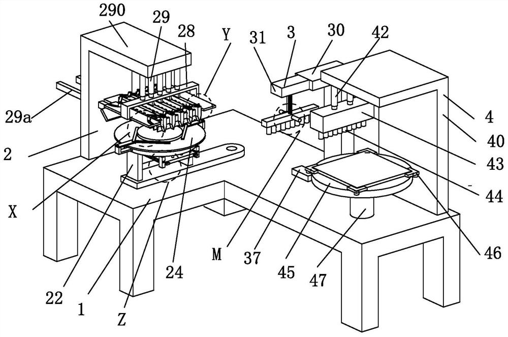
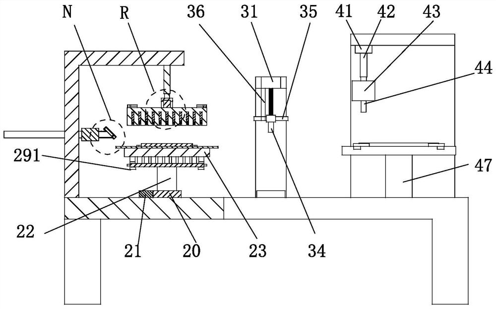
[0047] A semiconductor packaging equipment, comprising an L-shaped table 1, a cutting mechanism 2, a take-off mechanism 3 and a mounting mechanism 4, the L-shaped table 1 is installed on an existing working ground, and the upper end of the left end of the L-shaped table 1 is provided with a Cutting mechanism 2, a take-off mechanism 3 is installed on the upper end of the right end of the L-shaped table 1, and a mounting mechanism 4 is arranged on the right side of the take-off mechanism 3. The mechanism 3, the mounting mechanism 4 and the cutting mechanism 2 are all perpendicular to each other.

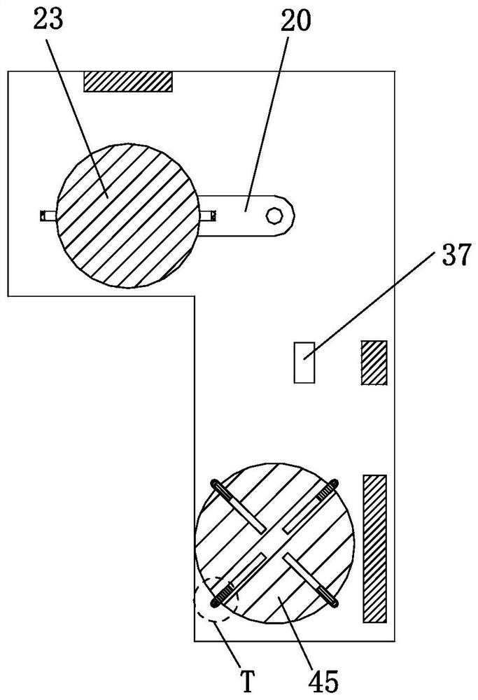
[0048] The cutting mechanism 2 includes a rotating plate 20, a No. 1 limit plate 21, a support plate 22, a disc 23, a blu...


PUM


Abstract

The invention relates to semiconductor packaging equipment and a packaging method. The equipment comprises an L-shaped table, a cutting mechanism, a taking mechanism and a surface mounting mechanism; the L-shaped table is installed on the existing working ground, the cutting mechanism is arranged at the upper end of the left end of the L-shaped table, the taking mechanism is installed at the upper end of the right end of the L-shaped table, and the surface mounting mechanism is arranged on the right side of the taking mechanism, and is installed on the upper end face of the right end of the L-shaped table; the taking mechanism and the mounting mechanism are perpendicular to the cutting mechanism. According to the semiconductor packaging equipment and the packaging method provided by the invention, semiconductor packaging is carried out by adopting a design concept of a linkage structure; the rapid semi-automatic conversion cooperation among the cutting mechanism, the taking mechanism and the mounting mechanism can greatly improve the semiconductor packaging efficiency and reduce the probability of manual errors, and a structure with the effect of absorbing and removing impurities generated by cutting is arranged to improve the cleaning degree of the surface of a wafer; therefore, the subsequent forming quality of the semiconductor can be improved.

Description

technical field [0001] The invention relates to the field of semiconductor processing, in particular to a semiconductor packaging device and a packaging method. Background technique [0002] Semiconductor refers to materials whose electrical conductivity is between conductors and insulators at room temperature. Semiconductor packaging refers to the process of processing wafers that have passed the test to obtain independent chips according to the product model and functional requirements. Testing, chip packaging and post-package testing, after the wafer is plasticized, a series of operations are also performed, such as post-curing, rib cutting and molding, electroplating, and printing processes. Semiconductors are used in integrated circuits, consumer electronics, communication systems, photovoltaic power generation, lighting. , high-power power conversion and other fields have applications, such as diodes are devices made of semiconductors, but the following problems will o...

Claims


Application Information

Patent Timeline
IPC IPC(8): H01L21/67H01L21/78H01L21/50H01L21/56
CPCH01L21/50H01L21/56H01L21/67092H01L21/67121H01L21/78
Inventor 不公告发明人
Owner 深圳芯闻科技有限公司
Why Eureka
Try Eureka