
Built-in encoding circuit and communication chip for communication chip

A communication chip and coding circuit technology, applied in the direction of logic circuit connection/interface layout, etc., can solve the problem of occupying MCU resources, etc., and achieve the effect of simple circuit structure and reduced occupancy.

Active Publication Date: 2021-07-27
SHANGHAI XINLONG SEMICON TECH CO LTD
View PDF3 Cites 0 Cited by
  • Summary
  • Abstract
  • Description
  • Claims
  • Application Information

AI Technical Summary

Problems solved by technology

The problem is that when dealing with some simple encoding requirements, MCU must also perform encoding, and then send the encoded signal to the communication chip for transmission. This transmission mode requires the support of MCU software and hardware, and often takes up MCU resources.

Method used


Image

  • Built-in encoding circuit and communication chip for communication chip
  • Built-in encoding circuit and communication chip for communication chip
  • Built-in encoding circuit and communication chip for communication chip

Examples


Embodiment Construction

[0031] In order to facilitate the understanding of those skilled in the art, the present invention will be further described in detail below in conjunction with specific embodiments.

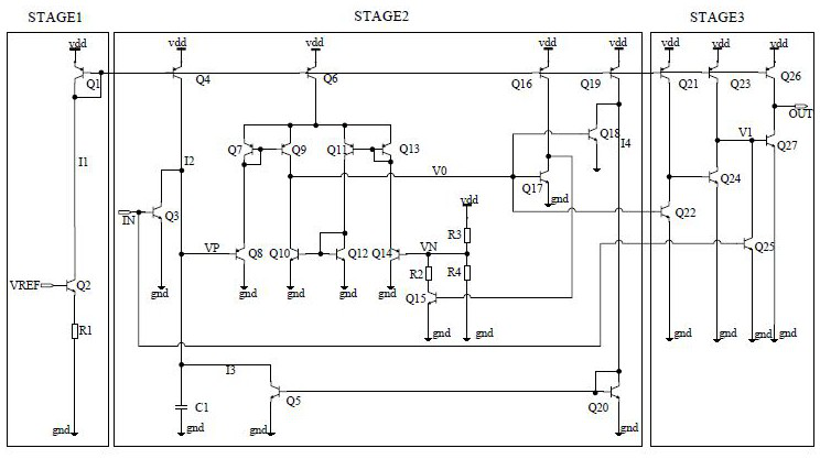
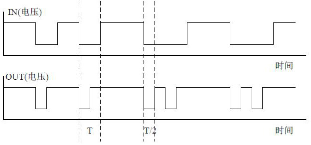
[0032] The embodiment of the present invention firstly provides a built-in coding circuit for a communication chip. The built-in coding circuit for a communication chip is a coding circuit realized by an integrated circuit manufacturing process using transistors, such as figure 1 As shown, it includes a reference circuit STAGE1, a rectangular wave generation circuit STAGE2, and a signal output circuit STAGE3 which are connected in sequence. The communication signal before encoding is input from the signal input terminal IN to the rectangular wave generation circuit STAGE2 and the signal output circuit STAGE3, and the signal encoded by the built-in encoding circuit used in the communication chip is output from the signal output terminal OUT; in addition, the reference circuit STAGE1, the rectangul...


PUM


Abstract

The invention provides a built-in coding circuit for a communication chip and a communication chip, and relates to the technical field of integrated circuit chips. The built-in coding circuit for a communication chip is realized by using an integrated circuit manufacturing process of a transistor, and its circuit structure is simple , has the function of automatically encoding the communication signals input by the signal input terminal, and can encode the communication signals of different rates by setting different frequencies in the communication chip, which reduces the design difficulty of the entire system and increases the reliability of the system. out of the MCU resources.

Description

technical field [0001] The invention relates to the technical field of integrated circuit chips, in particular to a built-in coding circuit for a communication chip and the communication chip. Background technique [0002] In the fields of air conditioning, security, smart home, etc., the communication between the host and the slave mostly adopts the Home BUS (referred to as HBS) communication protocol. The protocol uses a polarity-insensitive twisted pair to connect the master and slave devices, and supports communication and power supply through the twisted pair. Taking the field of central air conditioning as an example, the indoor unit of the central air conditioner supplies power to and communicates with the wire controller through twisted pair wires. The communication distance between the indoor unit and the wire controller is generally about 50m, but in a large shopping mall or office building, one wire controller needs to control multiple indoor units, and the longe...

Claims


Application Information

Patent Timeline
Patent Type & Authority Patents(China)
IPC IPC(8): H03K19/0175
CPCH03K19/0175
Inventor 贾生龙李瑞平
Owner SHANGHAI XINLONG SEMICON TECH CO LTD
Learn More