High-efficiency packaging equipment and packaging method for large-scale integrated circuit chips

A large-scale integrated circuit and packaging equipment technology, which is applied in packaging, transportation packaging, transportation and packaging, etc., can solve the problems of slow packaging speed, easy damage to the surface skin of fingers, and easy wear and tear of fingerprints on the surface of the thumb, so as to improve the accuracy of delivery , improve delivery efficiency, and avoid the effect of over-catch

Active Publication Date: 2021-06-15
COSMOS WEALTH
View PDF16 Cites 1 Cited by
  • Summary
  • Abstract
  • Description
  • Claims
  • Application Information

AI Technical Summary

Problems solved by technology

[0006] Two, in view of the problems in the prior art, the object of the present invention is to provide a kind of large-scale integrated circuit chip high-efficiency packaging equipment and packaging method, to solve the existing, when the circuit chip is packaged, it is necessary to manually take the packaging material manually, manually After taking it manually, you need to push the opening of the packaging bag with your thumb to open the opening of the packaging bag. When you manually use your thumb to frequently push the opening of the packaging bag to open, the fingerprint on the surface of the thumb is easy to wear, and the surface of the finger is easy to be damaged if you push frequently for a long time Skin, and the opening of each packaging bag is manually pushed open to make the operation efficient and the technical problem of slow packaging speed

Method used


Image

  • High-efficiency packaging equipment and packaging method for large-scale integrated circuit chips
  • High-efficiency packaging equipment and packaging method for large-scale integrated circuit chips
  • High-efficiency packaging equipment and packaging method for large-scale integrated circuit chips

Examples


Embodiment Construction

[0050] In order to make the technical means, creative features, goals and effects achieved by the present invention easy to understand, the present invention will be further elaborated below in conjunction with specific drawings. It should be noted that, in the case of no conflict, the embodiments and Features in the embodiments can be combined with each other.

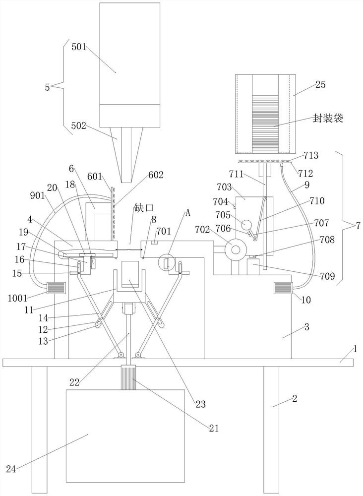
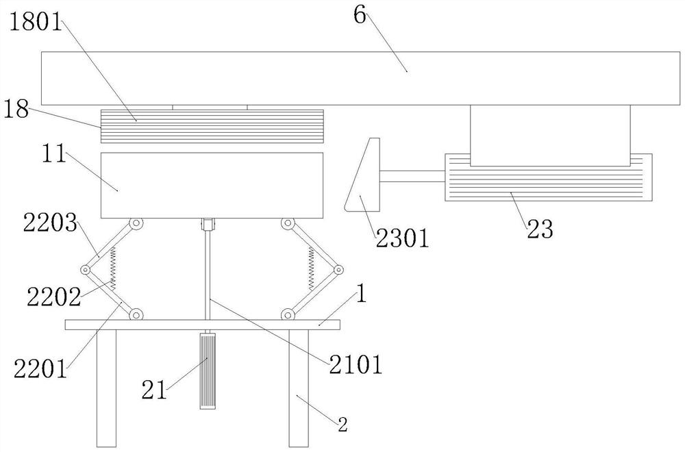
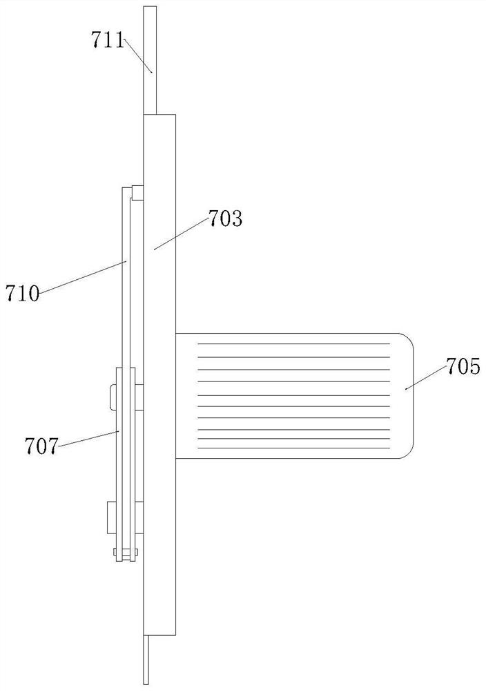
[0051] see Figure 1-9 It is a schematic diagram of the overall structure of a large-scale integrated circuit chip high-efficiency packaging equipment and packaging method;

[0052] A large-scale integrated circuit chip high-efficiency packaging equipment, including a workbench 1, which is placed horizontally, the bottom end of the workbench 1 is fixed with a support leg 2 standing on the ground, and the top left side of the workbench 1 is fixed with a The left support frame 4, the right support frame 3 is fixed on the right side of the top of the workbench 1, the left support frame 4 is set as an L-shaped plate stru...


PUM


Abstract

The invention provides an high-efficient packaging equipment and packing method for large-scale integrated circuit chips, and relates to the technical field of circuit chip production and packaging. The high-efficient packaging equipment comprises a workbench, a left supporting frame is fixedly arranged on the left side of the top end of the workbench, a right supporting frame is fixedly arranged on the right side of the top end of the workbench, the left supporting frame is of an L-shaped plate structure, the right supporting frame is of an L-shaped plate structure, the top face of the left supporting frame and the top face of the right supporting frame are equal in height, and a notch is formed between the left supporting frame and the right supporting frame. According to the high-efficiency packaging equipment and packaging method for the large-scale integrated circuit chip, through cooperation of a second electric push rod and a second servo motor, one packaging bag is taken out downwards from a material taking opening, the taken-out packaging bag extends into the position of a first suction cup, the top of the packaging bag is opened through cooperation of a first air suction pump and a second air suction pump, therefore, the large-scale circuit chips can be quickly and accurately put into the packaging bag through a feeding nozzle, the putting efficiency is improved, and the putting accuracy is improved.

Description

technical field [0001] The invention relates to the technical field of circuit chip production and packaging, in particular to a large-scale integrated circuit chip high-efficiency packaging equipment and packaging method. Background technique [0002] Large-scale integrated circuit chips, also known as large-scale integrated circuit boards, usually refer to logic gates with 100 to 9999 gates (or 1,000 to 99,999 components), and more than 1,000 electronic components assembled on one chip integrated circuit. An integrated circuit (integrated circuit, called an integrated circuit in Hong Kong and Taiwan) is a microelectronic device or component. Using a certain process, the transistors, diodes, resistors, capacitors, inductors and other components required in a circuit are interconnected together, fabricated on a small or several small semiconductor wafers or dielectric substrates, and then packaged in a tube. Inside the shell, it becomes a microstructure with the required c...

Claims


Application Information

Patent Timeline
Patent Type & Authority Applications(China)
IPC IPC(8): B65B5/10B65B7/02B65B43/18B65B43/30B65B43/46B65B43/54B65B51/10
CPCB65B5/101B65B7/02B65B43/18B65B43/30B65B43/465B65B43/54B65B51/10
Inventor 梅虞进
Owner COSMOS WEALTH
Why Eureka
Try Eureka