Supercharge Your Innovation With Domain-Expert AI Agents!

PCB metallization half-hole processing technology

A metallized semi-hole and processing technology, which is applied in the direction of the electrical connection of printed components, can solve the problems of extrusion and drawing, and can not be completely removed, so as to improve the appearance quality

Active Publication Date: 2021-06-15
江西红板科技股份有限公司
View PDF5 Cites 0 Cited by
  • Summary
  • Abstract
  • Description
  • Claims
  • Application Information

AI Technical Summary

Problems solved by technology

However, due to the fixed cutting direction of the milling machine, and the fineness and toughness of the glass fiber and the good ductility of copper, when the milling cutter moves to half the hole, the glass fiber and copper have no focus and will be squeezed to half. The wire drawing phenomenon in the hole cannot be completely removed

Method used


Image

  • PCB metallization half-hole processing technology

Examples


Embodiment Construction

[0019] In order to make the technical solution of the present invention more clearly expressed, the present invention will be further described below in conjunction with the accompanying drawings.

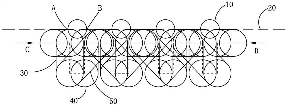
[0020] Such as figure 1 As shown, the present invention provides a kind of PCB metallization half hole processing technology, is used for processing the half hole of PCB board limit, and described half hole vertically runs through PCB, and PCB metallization half hole processing technology comprises the following steps:

[0021] (1), select the PCB core board, the PCB core board includes an insulating layer and two copper-clad laminates fixed on both sides of the insulating layer;

[0022] (2), the inner layer circuit, etch the inner layer circuit on the copper clad laminate on the PCB core board;

[0023] (3) Pressing, pressing the outer layer board to the inner core board to form a PCB mother board, the PCB mother board includes the effective area of ​​the PCB and the waste edge ...


PUM


Abstract

The invention relates to a PCB metallization half-hole processing technology. The technology comprises the following steps: (1) selecting a PCB core board; (2) selecting an inner layer circuit; (3) laminating: laminating the outer layer board on the inner layer core board to form a PCB mother board, and forming a junction line between the effective area of the PCB and the waste edge area of the PCB; (4) drilling: drilling a round hole in the PCB mother board; (5) metalizing the hole wall: electroplating a copper layer on the hole wall of the circular hole, and further metalizing the hole wall of the circular hole; (6) performing outer layer circuit etching: etching the outer layer circuit on the outer layer board; and (7) milling the board with a forward and reverse rotation forming machine: selecting a milling machine with the forward and reverse rotation function, and milling holes in the PCB mother board to form half holes. During half-hole machining, inner groove rough milling, forward blade fine trimming and reverse blade fine trimming machining treatment are sequentially carried out. The key problem that no acting point exists when a half-hole-opening milling cutter cuts glass fibers and copper is effectively solved, through the forward and reverse rotation board milling mode, forward blade board milling forming is carried out, and glass fiber and copper wire drawing is eliminated through reverse blade finishing, so the product appearance quality is improved.

Description

technical field [0001] The invention relates to a circuit board manufacturing process, in particular to a PCB metallized half-hole processing process. Background technique [0002] The metallized half hole of a normal PCB is drilled into a full round hole during drilling, then metallized by electroplating, and then half of the metallized hole is obtained by milling off. However, due to the fixed cutting direction of the milling machine, and the fineness and toughness of the glass fiber and the good ductility of copper, when the milling cutter moves to half the hole, the glass fiber and copper have no focus and will be squeezed to half. The wire drawing phenomenon in the hole cannot be completely removed. Contents of the invention [0003] Therefore, aiming at the deficiencies of the prior art, the object of the present invention is to provide a PCB metallization half-hole processing technology. [0004] A PCB metallization half-hole processing technology, comprising the ...

Claims


Application Information

Patent Timeline
IPC IPC(8): H05K3/42
CPCH05K3/42
Inventor 郭达文曾龙文伟峰刘长松谢世坤
Owner 江西红板科技股份有限公司
Features
  • R&D
  • Intellectual Property
  • Life Sciences
  • Materials
  • Tech Scout
  • Unparalleled Data Quality
  • Higher Quality Content
  • 60% Fewer Hallucinations
Learn More