Pin access method in integrated circuit layout wiring and device thereof

An integrated circuit and access method technology, which is applied in the fields of electrical digital data processing, special data processing applications, instruments, etc., can solve the problems of lack of back-end wiring global consideration, inability to complete detailed wiring of processes, and high calculation overhead. Improve efficiency and wiring success rate, improve wiring success rate, and the effect of balanced wiring distribution

Pending Publication Date: 2021-06-18
上海伴芯科技有限公司
View PDF0 Cites 2 Cited by
  • Summary
  • Abstract
  • Description
  • Claims
  • Application Information

AI Technical Summary

Problems solved by technology

[0005] The existing pin access schemes have the following two major problems: (1) Lack of global consideration of the entire back-end wiring, only considering the local issues of pin access, so many times it will lead to even if the local pin access seems to be successful, However, the detailed routing (Detail Route) behind the process cannot be completed; (2) Usually pin access is performed on the grid, and special processing must be done for pins that are not on the grid, and the calculation overhead is very large, even pins It can't come out at all, which leads to the failure of the entire wiring

Method used


Image

  • Pin access method in integrated circuit layout wiring and device thereof
  • Pin access method in integrated circuit layout wiring and device thereof
  • Pin access method in integrated circuit layout wiring and device thereof

Examples


Embodiment Construction

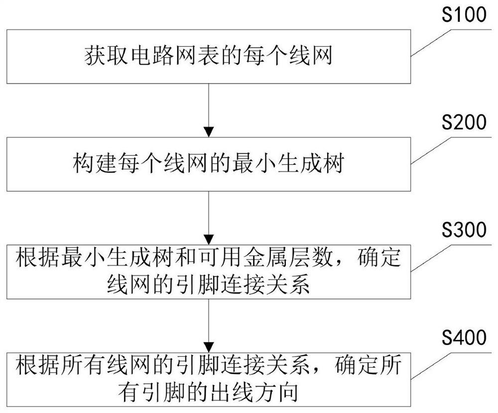
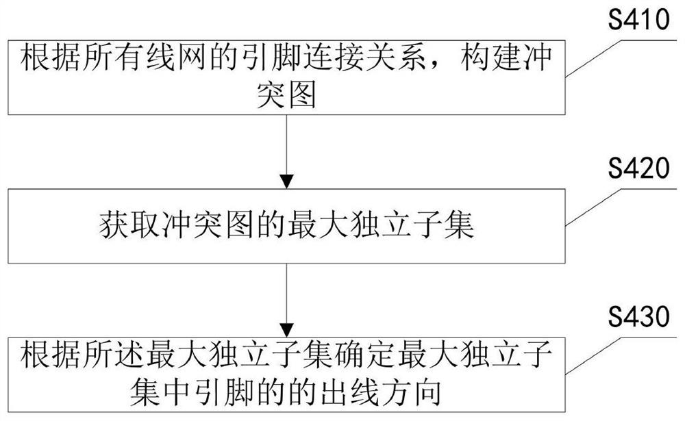
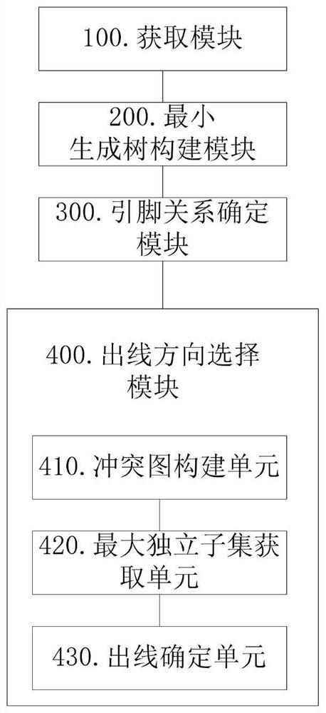
[0039] In order to more clearly describe the embodiments of the present invention or the technical solutions in the prior art, the specific embodiments of the present invention will be described below with reference to the accompanying drawings. Obviously, the accompanying drawings in the following description are only some embodiments of the present invention. For those of ordinary skill in the art, other drawings can also be obtained from these drawings without creative efforts, and obtain other implementations.

[0040] In order to keep the drawings concise, the drawings only schematically show the parts related to the present invention, and they do not represent its actual structure as a product. In addition, in order to make the drawings concise and easy to understand, only one of the components having the same structure or function in some drawings is schematically drawn, or only one of them is marked. As used herein, "one" not only means "only one", but also "more than...


PUM


Abstract

The invention provides a pin access method in integrated circuit layout wiring and a device thereof. The method comprises the following steps: acquiring each net of a circuit net list; constructing a minimum spanning tree of each line network; according to the minimum spanning tree and the number of available metal layers, determining the pin connection relation of the wire net, wherein the pin connection relation of the wire net comprises which pins are connected and which metal layer is connected; and according to the pin connection relationship of all the wire nets, determining the wire outlet directions of all the pins. According to the method, chip PPA optimization of a traditional algorithm is not taken as a target, the target serves full automation and completeness of the process of chip back-end physical design, a pin access scheme is globally considered and designed before specific wiring, and the wiring success rate and the pin access efficiency can be improved.

Description

technical field [0001] The invention relates to the technical field of EDA design, in particular to a method and device for accessing pins in the layout and wiring of an integrated circuit. Background technique [0002] Integrated circuit (IC, also known as chip) design includes chip front-end design and back-end design. The front-end design of the chip generates the logic netlist of the circuit, and the back-end design uses the EDA (Electronic Design Automation) design tool for layout, routing and physical verification, and finally generates GDSII data for manufacturing. [0003] Layouts are used to assign physical locations to standard cells, macroblocks, etc. on the layout. After placement comes routing. Routing is used to determine the exact design of the wiring required to connect these standard cells, macroblocks. The routing step implements all required connections while following the rules and constraints of the manufacturing process. [0004] With the advancemen...

Claims


Application Information

Patent Timeline
Patent Type & Authority Applications(China)
IPC IPC(8): G06F30/394
CPCG06F30/394
Inventor 周海李邦祥
Owner 上海伴芯科技有限公司
Why Eureka
Try Eureka