IC radio frequency antenna packaging structure manufacturing method and IC radio frequency antenna packaging structure

A packaging structure, radio frequency antenna technology, applied in the direction of antenna support/mounting device, antenna, antenna parts, etc., can solve the problem that the directional transmission of antenna signals cannot be realized, and achieve the effect of simple packaging structure

Active Publication Date: 2021-06-18
FOREHOPE ELECTRONICS NINGBO CO LTD
View PDF6 Cites 0 Cited by
  • Summary
  • Abstract
  • Description
  • Claims
  • Application Information

AI Technical Summary

Problems solved by technology

The IC radio frequency antenna structure in the prior art can

Method used


Image

  • IC radio frequency antenna packaging structure manufacturing method and IC radio frequency antenna packaging structure
  • IC radio frequency antenna packaging structure manufacturing method and IC radio frequency antenna packaging structure
  • IC radio frequency antenna packaging structure manufacturing method and IC radio frequency antenna packaging structure

Examples


Example

[0054] first embodiment

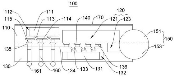
[0055] Please refer to figure 1 , An IC radio frequency antenna packaging structure 100 provided by an embodiment of the present invention includes a first packaging member 110 , a second packaging member 130 , a functional chip 111 , a radio frequency chip 131 and an antenna 140 . The first package 110 is provided with a first RDL circuit 114 , the second package 130 is provided with a second RDL circuit 134 , and the function chip 111 is arranged in the first package 110 and is electrically connected to the first RDL circuit 114 . The chip 131 is disposed in the second package 130 and is electrically connected to the second RDL line 134 , the first RDL line 114 is electrically connected to the second RDL line 134 , and the antenna 140 is electrically connected to the second RDL line 134 ; the first package 110 A first hemisphere 151 is provided thereon, a second hemisphere 153 is provided on the second package 130 , and the dielectric constant of t...

Example

[0060] Second Embodiment

[0061] refer to Figure 2 to Figure 10 , and combine figure 1 , the embodiment of the present invention provides a method for manufacturing an IC radio frequency antenna packaging structure 100, which mainly includes the following steps:

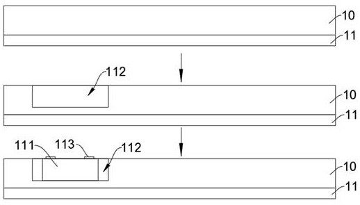
[0062] S10: Fabricating the first package 110 .

[0063] Please refer to figure 2 and image 3 , the first base material 10 is provided, and the function chip 111 is mounted on the first base material 10 . Optionally, the first substrate 10 is placed on the first carrier 11, and the first substrate 10 can be made of silicon, silicon dioxide, or polymer materials, and the warpage during the manufacturing process can be eliminated by using the first carrier 11 For the problem of curvature, the material of the first carrier 11 may be glass, silicon oxide, metal or other materials. In this embodiment, a laser is used to open grooves on the first base material 10 , and a first mounting groove 112 is formed on the...


PUM


Abstract

The invention provides an IC radio frequency antenna packaging structure manufacturing method and an IC radio frequency antenna packaging structure and relates to the technical field of semiconductor packaging. The manufacturing method comprises the following steps of respectively providing a first substrate and a second substrate, mounting a functional chip on the first substrate, forming a first hemispherical groove in the first substrate, and arranging a first dielectric layer in the first hemispherical groove to form a first packaging piece; mounting a radio frequency chip on the second base material, and performing plastic package and exposing a second line bonding pad of the radio frequency chip; arranging a radio frequency connection end on the second line bonding pad; an antenna being arranged at the radio frequency connection end; a second hemispherical groove being formed in the second base material, a second dielectric layer being arranged in the second hemispherical groove, and a second packaging piece being formed; and pressing the first packaging piece and the second packaging piece to enable the notch of the first hemispherical groove and the notch of the second hemispherical groove to be oppositely combined into a sphere, so a signal of the antenna is transmitted outwards through the sphere, and directional transmission of the signal of the antenna is realized.

Description

technical field [0001] The present invention relates to the technical field of semiconductor packaging, and in particular, to a manufacturing method of an IC radio frequency antenna packaging structure and an IC radio frequency antenna packaging structure. Background technique [0002] With the rapid development of the semiconductor industry, IC RF antenna structures are widely used in the semiconductor industry. Integrated antennas include Antenna-on-Chip (AoC) and Antenna-in-Package (AiP) ) two types. With the iteration of electronic products used in high-frequency and low-frequency signals in the field of communication, electronic products are required to have antenna functions to meet their high-frequency or low-frequency signal transmission. This requires IC RF antenna signals in electronic products to be able to transmit in a specified direction. The IC radio frequency antenna structure in the prior art cannot realize the directional transmission of the antenna signal...

Claims


Application Information

Patent Timeline
IPC IPC(8): H01L21/50H01L21/56H01L23/66H01Q1/22
CPCH01L21/50H01L21/568H01L23/66H01L2223/6677H01Q1/2283
Inventor 吴春悦钟磊何正鸿
Owner FOREHOPE ELECTRONICS NINGBO CO LTD
Why Eureka
Try Eureka