Electromagnetic shielding structure manufacturing process and electromagnetic shielding structure

A technology of electromagnetic shielding structure and manufacturing process, applied in circuits, electrical components, electric solid devices, etc., can solve the problems of short circuit of grounding shielding wires, affecting product quality, and failure of electromagnetic shielding performance of products, and achieving easy connection and electromagnetic shielding functions. The effect of stable and stable electromagnetic shielding effect

Active Publication Date: 2021-08-06
FOREHOPE ELECTRONICS NINGBO CO LTD
View PDF4 Cites 0 Cited by
  • Summary
  • Abstract
  • Description
  • Claims
  • Application Information

AI Technical Summary

Problems solved by technology

[0003] In this kind of manufacturing process, cutting deviation is likely to occur during the cutting process, resulting in a short circuit of the grounding shielding wire, which leads to the failure of the electromagnetic shielding performance of the product and affects product quality.

Method used


Image

  • Electromagnetic shielding structure manufacturing process and electromagnetic shielding structure
  • Electromagnetic shielding structure manufacturing process and electromagnetic shielding structure
  • Electromagnetic shielding structure manufacturing process and electromagnetic shielding structure

Examples


no. 1 example

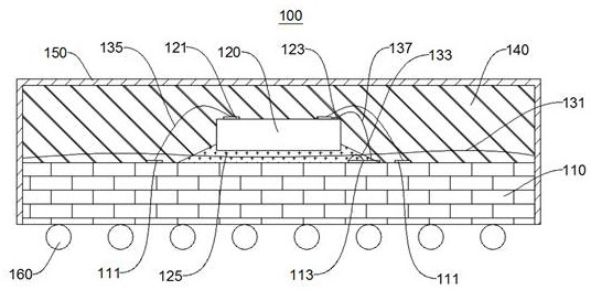
[0055] Please refer to figure 1 and figure 2 , in order to effectively prevent the electromagnetic interference generated by various chips 120 and components, an electromagnetic shielding structure 100 provided in an embodiment of the present invention includes a substrate 110 , a chip 120 , a plastic package 140 and a metal layer 150 . A first pad 111, a second pad 113, and a plurality of third pads 115 are arranged at intervals on the substrate 110, and the first pad 111 and the second pad 113 are located in the enclosed space formed by the plurality of third pads 115. Inside; a first connection line 131 with a grounding property is provided between the plurality of third pads 115 , and the chip 120 is located on the first connection line 131 . The chip 120 is electrically connected to the first pad 111 to realize the functional connection between the chip 120 and the substrate 110; the chip 120 is electrically connected to the second pad 113 to realize the grounding of th...

no. 2 example

[0062] Please refer to Figure 3 to Figure 10 , the embodiment of the present invention provides a manufacturing process of the electromagnetic shielding structure 100, the main steps of which include:

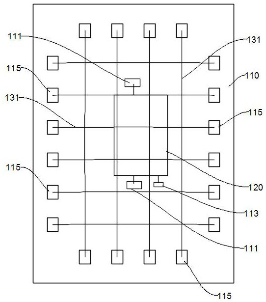
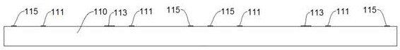
[0063] A substrate 110 is provided, and a first pad 111, a second pad 113, and a plurality of third pads 115 are formed on the substrate 110, wherein the number of the first pads 111 corresponds to the number of functional pads 121 on the chip 120, The first pad 111 is used to realize the functional connection of the chip 120, the second pad 113 is used to realize the grounding of the chip 120, and a plurality of third pads 115 are arranged at intervals and connect the chip 120, the first pad 111 and the second pad to each other. A disc 113 surrounds it. It should be noted that the first bonding pad 111 and the second bonding pad 113 are respectively arranged around the chip 120, and the third bonding pad 115 can be arranged on opposite sides of the chip 120 or around the chi...


PUM


Abstract

The application provides an electromagnetic shielding structure manufacturing process and an electromagnetic shielding structure, which relate to the technical field of semiconductor packaging. The manufacturing process of the electromagnetic shielding structure includes forming a first bonding pad, a second bonding pad and a plurality of third bonding pads on the substrate, wherein the plurality of third bonding pads are arranged at intervals and surround the first bonding pad and the second bonding pad ; between the third pads, the first connection wires with grounding properties are arranged in a staggered distribution; the chip is mounted on the substrate; wherein, the chips are respectively electrically connected to the first pad and the second pad, and are located at the first connection online; form a plastic package on the substrate, and plant balls on the side of the substrate away from the plastic package; cut the plastic package and the substrate along the dicing line to form a single product; wherein, the dicing line is located on the third pad close to the chip side, so that the first connection line is exposed from the side of the plastic package after cutting; a metal layer is formed on the surface of the plastic package of a single product, so that the metal layer is electrically connected to the first connection line, and a good electromagnetic shielding effect is achieved.

Description

technical field [0001] The present invention relates to the technical field of semiconductor packaging, in particular to a manufacturing process of an electromagnetic shielding structure and an electromagnetic shielding structure. Background technique [0002] In the existing system-level package module electromagnetic shielding technology, the grounding wire is usually arranged on the edge of the substrate cutting line. After the cutting process, a single product is formed, and then the film is applied to the back of the single product substrate and metal sputtering is performed to achieve the grounding wire. It communicates with the metal layer circuit to realize the electromagnetic shielding effect of the product. [0003] In this manufacturing process, cutting deviation is likely to occur during the cutting process, resulting in a short circuit of the grounding shielding wire, which leads to failure of the electromagnetic shielding performance of the product and affects ...

Claims


Application Information

Patent Timeline
Patent Type & Authority Patents(China)
IPC IPC(8): H01L21/60H01L23/552
CPCH01L24/85H01L23/552H01L2224/97H01L2224/73265H01L2224/32225H01L2224/48227H01L2224/92247H01L2224/8592H01L2924/15311H01L2924/181H01L2924/00012H01L2924/00
Inventor 包宇君李利何正鸿
Owner FOREHOPE ELECTRONICS NINGBO CO LTD
Why Eureka
Try Eureka