Composite substrate for packaging high-speed laser chip

A technology of chip packaging and composite substrates, applied in lasers, laser components, semiconductor lasers, etc., can solve problems such as difficulties in making through holes, meet the requirements of high-frequency transmission, realize the grounding function, and meet the effects of heat dissipation requirements

Pending Publication Date: 2022-07-22
上海矽安光电科技有限公司
View PDF0 Cites 0 Cited by
  • Summary
  • Abstract
  • Description
  • Claims
  • Application Information

AI Technical Summary

Problems solved by technology

However, when the transmission signal is higher than 30GHZ, a multi-layer aluminum nitride substrate is required, and each layer requires through holes and electroplating to realize interlayer interconnection. Aluminum nitride is also a high-hardness material, and it is difficult to make through holes

Method used


Image

  • Composite substrate for packaging high-speed laser chip
  • Composite substrate for packaging high-speed laser chip

Examples


Embodiment Construction

[0020] The technical solutions in the embodiments of the present application will be clearly and completely described below with reference to the drawings in the embodiments of the present application. Obviously, the described embodiments are only a part of the embodiments of the present application, but not all of the embodiments. Based on the embodiments in the present application, all other embodiments obtained by those of ordinary skill in the art without creative efforts shall fall within the protection scope of the present application.

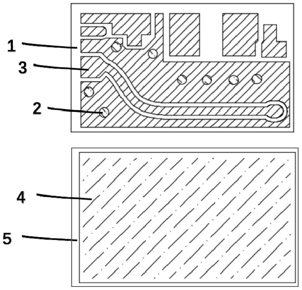
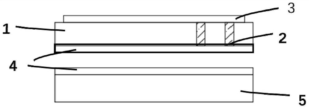
[0021] like figure 1 and figure 2 As shown, in one embodiment of the present application, a composite substrate for high-speed laser chip packaging includes: a substrate 1, a coplanar waveguide structure 3 and a low-resistance silicon wafer 5, and a surface of the substrate 1 is provided with a coplanar waveguide Structure 3, wherein the coplanar waveguide structure 3 is prefabricated with through holes 2; In this embodiment, only one...


PUM

PropertyMeasurementUnit
thicknessaaaaaaaaaa
thicknessaaaaaaaaaa
thicknessaaaaaaaaaa

Abstract

The invention discloses a composite substrate for packaging a high-speed laser chip, which comprises a substrate, a coplanar waveguide structure and a low-resistance silicon wafer, and is characterized in that the coplanar waveguide structure is arranged on the surface of the substrate, and a through hole is prefabricated in the coplanar waveguide structure; a first metal layer is plated on the back surface of the substrate, and the low-resistance silicon wafer is bonded with the substrate. Compared with sintering and punching of multiple layers of ceramics in the prior art, only one layer of thin substrate is adopted, the heat dissipation requirement can be met, the high-frequency transmission requirement can also be met, the low-resistance silicon wafer at the bottom serves as a conductor, and the grounding function can be achieved.

Description

technical field [0001] The application belongs to the technical field of optoelectronic devices, and in particular relates to a composite substrate for high-speed laser chip packaging. Background technique [0002] In optical fiber communication technology, semiconductor lasers are mainly used as signal sources. With the continuous improvement of laser chip fabrication technology, not only the cost of the laser chip is greatly reduced, but also the modulation frequency of a single laser chip has reached 10GHZ or even dozens of GHZ. At present, the key factor restricting the characteristics and cost of the signal source mainly lies in the packaging technology. In the packaging process, the packaging substrate must provide high-frequency signals to the laser, and at the same time meet the requirements of laser heat dissipation. Due to its high thermal conductivity and low dielectric loss, aluminum nitride ceramics are widely used in optical communication laser packaging and ...

Claims


Application Information

Patent Timeline
Patent Type & Authority Applications(China)
IPC IPC(8): H01S5/02315H01S5/0225H01S5/0239H01S5/024
CPCH01S5/02315H01S5/0225H01S5/0239H01S5/02461
Inventor 徐建卫汪鹏
Owner 上海矽安光电科技有限公司
Why Eureka
Try Eureka