Storage system for controlling SATA (Serial Advanced Technology Attachment) disk based on NVME protocol
A storage system and protocol control technology, applied in the input/output process of data processing, instruments, electrical digital data processing, etc., can solve the requirements of high standards, high customization and scalability, security and Poor flexibility, easy damage and other problems, to achieve the effect of easy to put into use, simple design, and improved safety
- Summary
- Abstract
- Description
- Claims
- Application Information
AI Technical Summary
Problems solved by technology
Method used
Image

Examples
Embodiment Construction
[0022] The following will clearly and completely describe the technical solutions in the embodiments of the application with reference to the drawings in the embodiments of the application. Apparently, the described embodiments are only some, not all, embodiments of the application. Based on the embodiments in this application, all other embodiments obtained by persons of ordinary skill in the art without making creative efforts belong to the scope of protection of this application.
[0023] It should be noted that, unless otherwise defined, all technical and scientific terms used herein have the same meaning as commonly understood by those skilled in the technical field of the application. The terms used herein in the description of the application are only for the purpose of describing specific embodiments, and are not intended to limit the application.
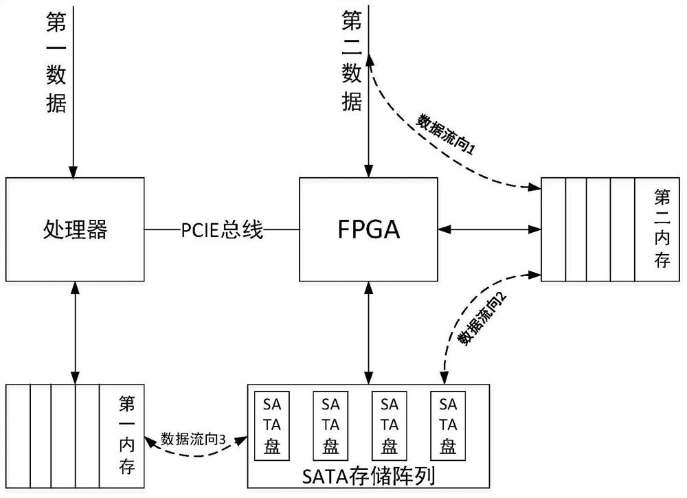
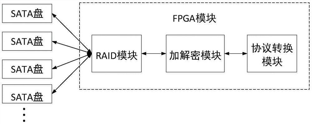
[0024] like Figure 1-2 As shown, a storage system for controlling SATA disks based on the NVME protocol includes a proc...
PUM
 Abstract
Description
Claims
Application Information
 - R&D
- Intellectual Property
- Life Sciences
- Materials
- Tech Scout
- Unparalleled Data Quality
- Higher Quality Content
- 60% Fewer Hallucinations
Browse by: Latest US Patents, China's latest patents, Technical Efficacy Thesaurus, Application Domain, Technology Topic, Popular Technical Reports.
© 2025 PatSnap. All rights reserved.Legal|Privacy policy|Modern Slavery Act Transparency Statement|Sitemap|About US| Contact US: help@patsnap.com