Optimization method of integrated circuit design data

A technology for design data and integrated circuits, applied in the field of optimization of integrated circuit design data, can solve the problems of complex integrated circuit design, long cycle, and high R&D costs, and achieve the effects of shortening the design cycle, less calculation, and reducing R&D costs

Pending Publication Date: 2021-06-29
XIDIAN UNIV
View PDF3 Cites 2 Cited by
  • Summary
  • Abstract
  • Description
  • Claims
  • Application Information

AI Technical Summary

Problems solved by technology

[0003] The purpose of the present invention is to provide a method for optimizing integrated circuit design data to solve the problems of complex, long cycle and high research and development costs in existing integrated circuit design

Method used


Image

  • Optimization method of integrated circuit design data
  • Optimization method of integrated circuit design data
  • Optimization method of integrated circuit design data

Examples


Embodiment

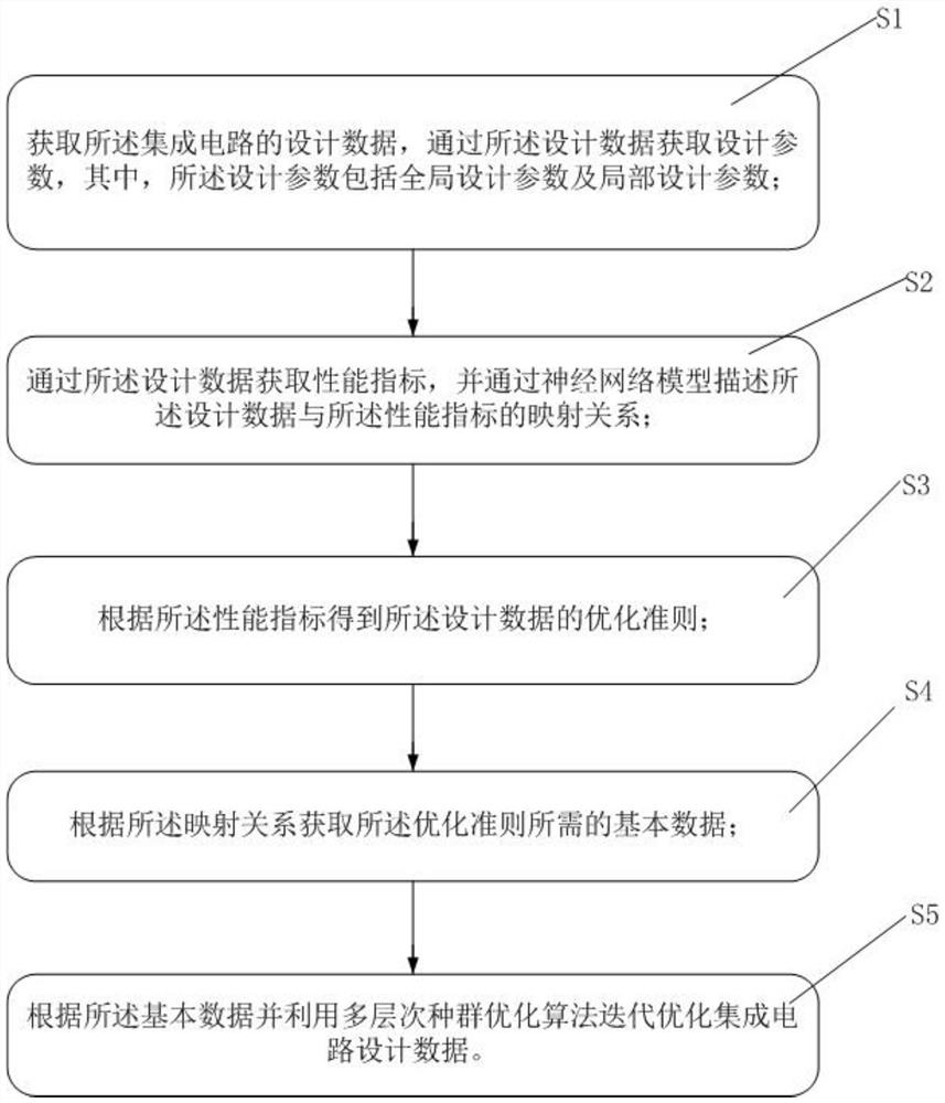
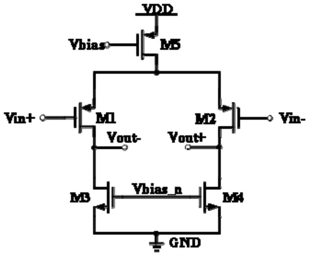
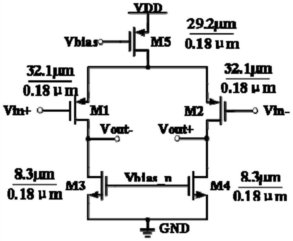
[0041] The present invention is a multi-level population optimization method for integrated circuit design parameters, the flow chart of which is shown in Figure 1. The PMOS input differential integrated circuit designed with NMOS current source as the load ( figure 2 ) as an example, the implementation details of the multi-level population optimization method of the integrated circuit design parameters involved in the present invention are introduced in detail, and the optimization method of the integrated circuit design data includes:

[0042] S1: Obtain design data of the integrated circuit, and obtain design parameters through the design data, wherein the design parameters include global design parameters and local design parameters;

[0043] In this embodiment, the design data of the PMOS input differential integrated circuit with the NMOS current source as the load is acquired by Cadence software combined with an orthogonal design method. Its design parameters are divi...


PUM


Abstract

The invention discloses an optimization method for design data of an integrated circuit, and the method comprises the steps: obtaining the design data of the integrated circuit, obtaining design parameters through the design data, and enabling the design parameters to comprise global design parameters and local design parameters; obtaining a performance index through the design data, and describing a mapping relation between the design data and the performance index through a neural network model; specifying an optimization criterion of the design data according to the performance index; obtaining basic data required by the optimization criterion according to the mapping relation; and iteratively optimizing integrated circuit design data by using a multi-level population optimization algorithm. According to the optimization method for the integrated circuit design data, the problems that an existing integrated circuit is complex in design, long in period and high in research and development cost can be solved.

Description

technical field [0001] The invention relates to the technical field of integrated circuit design, in particular to a method for optimizing integrated circuit design data. Background technique [0002] Integrated circuits, also known as microcircuits, microchips, chips / chips. There are many parameters in IC design, and the design process is complicated. It needs to rely on the experience of R&D personnel for repeated trial and error adjustments to obtain the desired performance indicators of circuit modules. This time-consuming and labor-intensive design method reduces the efficiency of IC design and increases R&D costs. , prolonging the development cycle of integrated circuit chips. Contents of the invention [0003] The object of the present invention is to provide a method for optimizing integrated circuit design data, so as to solve the existing problems of complex integrated circuit design, long cycle and high research and development costs. [0004] The technical sc...

Claims


Application Information

Patent Timeline
Patent Type & Authority Applications(China)
IPC IPC(8): G06F30/3308G06N3/00G06N3/04G06N3/08
CPCG06F30/3308G06N3/006G06N3/04G06N3/08
Inventor 谌东东李迪张启东杨银堂
Owner XIDIAN UNIV
Why Eureka
Try Eureka