Supercharge Your Innovation With Domain-Expert AI Agents!

Semiconductor device and manufacturing method

A technology of semiconductors and devices, applied in the field of power semiconductor devices, can solve the problems of the development needs of high-density integrated circuits with too large PN junction isolation area, and achieve the effect of improving the utilization rate and reducing the cost

Active Publication Date: 2021-07-02
WUXI NCE POWER
View PDF9 Cites 0 Cited by
  • Summary
  • Abstract
  • Description
  • Claims
  • Application Information

AI Technical Summary

Problems solved by technology

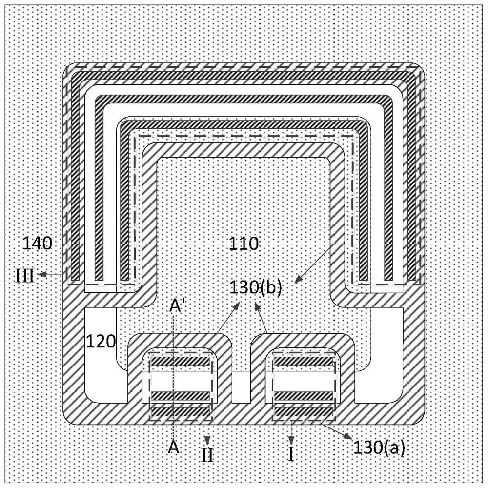
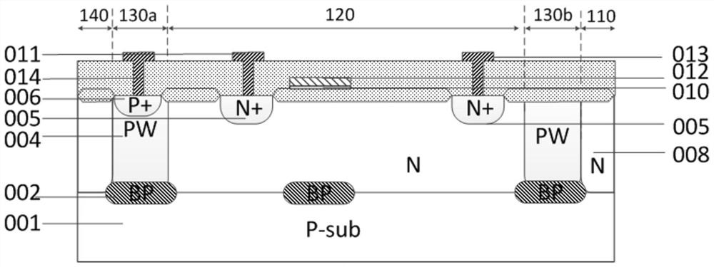
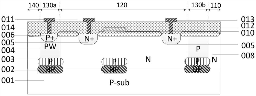
[0005] The purpose of the present invention is to overcome the problem that the PN junction isolation occupation area existing in the prior art is too large and the development of integrated circuit high density needs to be contradictory, and to provide a new type of Semiconductor device, the device of the present invention can make full use of the high and low voltage junction terminal area to prepare various power devices, improve the utilization rate of the chip area, increase the density of the integrated circuit, thereby reducing the cost of the integrated circuit

Method used


Image

  • Semiconductor device and manufacturing method
  • Semiconductor device and manufacturing method
  • Semiconductor device and manufacturing method

Examples


Embodiment Construction

[0047] In order to make the object, technical solution and advantages of the present invention clearer, the present invention will be further described in detail below in conjunction with the accompanying drawings and embodiments. It should be understood that the specific embodiments described here are only used to explain the present invention, not to limit the present invention.

[0048] It should be noted that, in the case of no conflict, the embodiments of the present invention and the features in the embodiments can be combined with each other. The present invention will be described in detail below with reference to the accompanying drawings and examples.

[0049] In order to enable those skilled in the art to better understand the solutions of the present invention, the following will clearly and completely describe the technical solutions in the embodiments of the present invention in conjunction with the accompanying drawings in the embodiments of the present inventio...


PUM


Abstract

The invention provides a semiconductor device, and the semiconductor device comprises a P-type substrate; an N-type doped epitaxial layer is arranged on the P-type substrate, a high-voltage region and a low-voltage region are arranged on the N-type doped epitaxial layer, a high-low voltage junction terminal region is arranged between the high-voltage region and the low-voltage region, a first P-type isolation column is arranged between the low-voltage region and the high-low voltage junction terminal region, a first P-type isolation column is arranged between the high-voltage region and the high-low voltage junction terminal region, a second P-type isolation column is arranged between the high-voltage region and the high-low voltage junction terminal region, the first P-type isolation column is connected with the second P-type isolation column, the first P-type isolation column and the second P-type isolation column form one or more closed regions, and high-voltage devices are arranged in the closed regions; the high-voltage devices are one or more of a JFET device, an LDMOS device, an LIGBT device and a power diode device. According to the invention, the utilization rate of the chip area is improved, so that the cost of an integrated circuit is reduced.

Description

technical field [0001] The invention relates to a semiconductor device, especially an easy-to-integrate power semiconductor device. Background technique [0002] With the rapid development of integrated circuit technology, integrated circuits are increasingly developing in the direction of high density, high performance, and high reliability. [0003] High density requires that a variety of different circuits and devices can be integrated in the integrated circuit, and the limited area of ​​the integrated circuit can be fully utilized to realize as many functions as possible. For integrated circuits, especially analog integrated circuits, the interior of the chip is generally divided into a high-voltage area, a low-voltage area, and a high-low voltage junction terminal area that isolates the high-voltage area and the low-voltage area. For some more complex analog circuits, due to the different operating voltages of each area, the entire chip will be divided into more voltag...

Claims


Application Information

Patent Timeline
IPC IPC(8): H01L29/06H01L27/02
CPCH01L29/0603H01L29/0615H01L29/0642H01L29/0684H01L27/0207H01L29/7393H01L29/66325
Inventor 朱袁正周锦程叶鹏杨卓刘晶晶
Owner WUXI NCE POWER
Features
  • R&D
  • Intellectual Property
  • Life Sciences
  • Materials
  • Tech Scout
  • Unparalleled Data Quality
  • Higher Quality Content
  • 60% Fewer Hallucinations
Learn More