Supercharge Your Innovation With Domain-Expert AI Agents!

A high-performance high-speed input buffer circuit

An input buffer circuit, high-speed technology, applied in the direction of logic circuit connection/interface layout, etc., can solve the problem that the input buffer circuit is difficult to meet, and achieve the effects of increasing bandwidth, increasing gain, and increasing flipping speed.

Active Publication Date: 2021-12-17
WUXI ESIONTECH CO LTD +1
View PDF6 Cites 0 Cited by
  • Summary
  • Abstract
  • Description
  • Claims
  • Application Information

AI Technical Summary

Problems solved by technology

figure 1 The input buffer circuit shown in the existing structure is difficult to meet this requirement

Method used


Image

  • A high-performance high-speed input buffer circuit
  • A high-performance high-speed input buffer circuit
  • A high-performance high-speed input buffer circuit

Examples


Embodiment Construction

[0041] The specific embodiments of the present invention will be further described below in conjunction with the accompanying drawings.

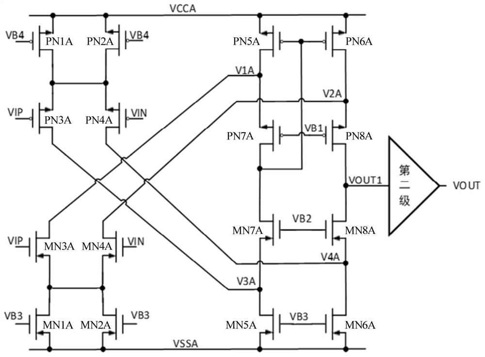
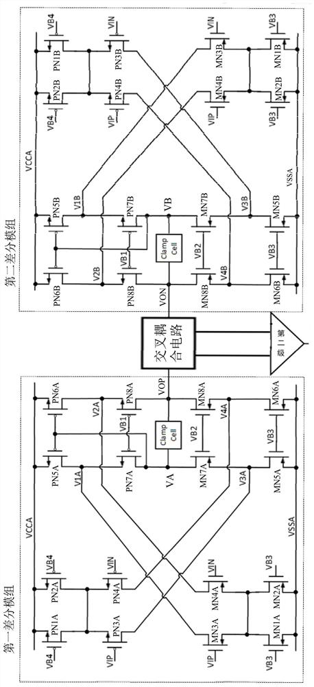
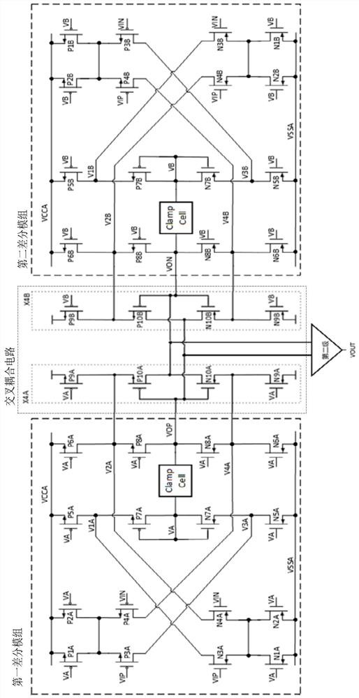
[0042] This application discloses a high-performance high-speed input buffer circuit, please refer to figure 2 , the high-speed input buffer circuit includes a first differential module, a second differential module and a cross-coupling circuit, the first differential module and the second differential module have the same structure, and each differential module includes a first differential amplifier circuit , the second differential amplifier circuit and the output module, wherein the first differential amplifier circuit is connected to the analog power supply VCCA and the two output terminals V1A and V2A are connected to the output module, the second differential amplifier circuit is connected to the analog ground VSSA and the two output terminals V3A and V4A Connect to output module. A pair of differential input signals VIN and VIP wit...


PUM


Abstract

The invention discloses a high-performance high-speed input buffer circuit, which relates to the field of circuit technology. The high-speed input buffer circuit is provided with an output clamping circuit at the differential output end of each differential module, and the differential output ends of two differential modules The output signal is cross-coupled by the cross-coupling circuit and then outputs a pair of differential output signals to the subsequent stage circuit. The output clamp circuit can make the output flip quickly, improve the bandwidth, and stabilize the output common-mode voltage at the same time, while the cross-coupling circuit improves gain, so that the high-speed input buffer circuit meets the dual requirements of bandwidth and gain.

Description

technical field [0001] The invention relates to the technical field of circuits, in particular to a high-performance high-speed input buffer circuit. Background technique [0002] When the signal is input from outside the chip, it needs to be received by the input buffer circuit, and the signal level is converted to the internal voltage domain level of the chip, so that the signal can be further processed. When designing an input buffer circuit, the following aspects need to be considered: [0003] 1. The level standard of the input signal, such as common mode level VCM, differential mode level VID, different level standards often define different VCM and VID ranges, if the input buffer circuit needs to be compatible with multiple level standards, for example Compatible with LVDS / DDR / MIPI applications, the possible VCM is 0.07V~1.8V, and the VID is 0.07V~1.8V. On the one hand, it is necessary to adopt a full-swing input circuit structure to realize the normal operation of ...

Claims


Application Information

Patent Timeline
Patent Type & Authority Patents(China)
IPC IPC(8): H03K19/0175
CPCH03K19/0175
Inventor 马锡昆谢宜政
Owner WUXI ESIONTECH CO LTD
Features
  • R&D
  • Intellectual Property
  • Life Sciences
  • Materials
  • Tech Scout
  • Unparalleled Data Quality
  • Higher Quality Content
  • 60% Fewer Hallucinations
Learn More