

Packaging structure and forming method thereof
A technology of packaging structure and molding method, which is applied in the manufacture of electrical components, electrical solid devices, semiconductor/solid devices, etc., can solve the problems of complex and cumbersome processes and high process requirements, simplify the packaging process, improve mass production efficiency and quantity produce a stabilizing effect
- Summary
- Abstract
- Description
- Claims
- Application Information
AI Technical Summary
Problems solved by technology
Method used
Image

Examples
Embodiment 1
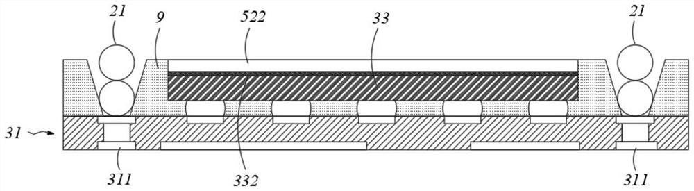
[0082] Such as Figure 11 As shown, in this packaging structure, the packaging module 3 is composed of a substrate 31 and a chip component 33, the chip component 33 is connected to the substrate 31 through solder balls, the substrate 31 is embedded with a pad, and the back of the chip component 33 is provided with heat sink.
[0083] The outer connecting frame structure 5 can be made of a metal structure through an integral molding process. The formed integrated outer connecting frame structure 5 includes a connecting beam 52 and metal pins extending vertically downward from both ends of the connecting beam 52. The metal pins can be Formed by bending the edge of the metal structure, it plays the role of supporting the connecting beam 52; the upper surface of the metal structure can be punched to form the connecting beam 52, so that the middle part of the connecting beam 52 is depressed downward to form a depression, and the connecting beam 52 The two ends protrude and arch up...
Embodiment 2
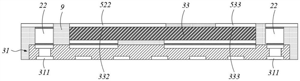
[0089] Such as Figure 12 As shown, similarly, in this package structure, the package module 3 is composed of a substrate 31 and a chip component 33 , the substrate 31 is embedded with pads, and the back of the chip component 33 is provided with a heat sink.
[0090] Different from the first embodiment, in this embodiment, an electrical connection portion is provided on the back of the chip component 33 , and the electrical connection portion and the heat dissipation portion are independent of each other. The electrical connection part is used as the third connection part 333 .
[0091]Correspondingly, the middle part of the connecting beam 52 of the outer connecting frame structure 5 is also recessed downward to form another concave part, so that all the concave parts and the connecting beams 52 between all the metal pins protrude and arch upward. The lower end of the concave portion is used as the third outer connecting portion 533 .
[0092] Similarly, glue is firstly dis...
PUM
 Abstract
Description
Claims
Application Information