Method for solving stress of thin substrate

A thin substrate and stress technology, applied in the field of solving the thin substrate stress, can solve the problems of measurement value fluctuation, limited light wave penetration depth, lack of precision, etc., to reduce the large stress fluctuation and accurately evaluate the thin substrate processing technology. Quality, the effect of improving continuity

Active Publication Date: 2021-07-23
HEFEI UNIV OF TECH
View PDF3 Cites 2 Cited by
  • Summary
  • Abstract
  • Description
  • Claims
  • Application Information

AI Technical Summary

Problems solved by technology

However, in actual measurement, the Raman frequency shift will still be affected by the focal depth, laser heating effect and other temperature, and it does not have very high precision in the absence of effective calibration criteria; and due to the limited penetration depth of light waves, the obtained is the best The stress state of the surface layer, the micro-Raman measurement results reflect the changes in the microstructure of the processing damage, and the fluctuations of the measured values ​​​​at different positions are relatively large

Method used


Image

  • Method for solving stress of thin substrate
  • Method for solving stress of thin substrate
  • Method for solving stress of thin substrate

Examples


Embodiment 1

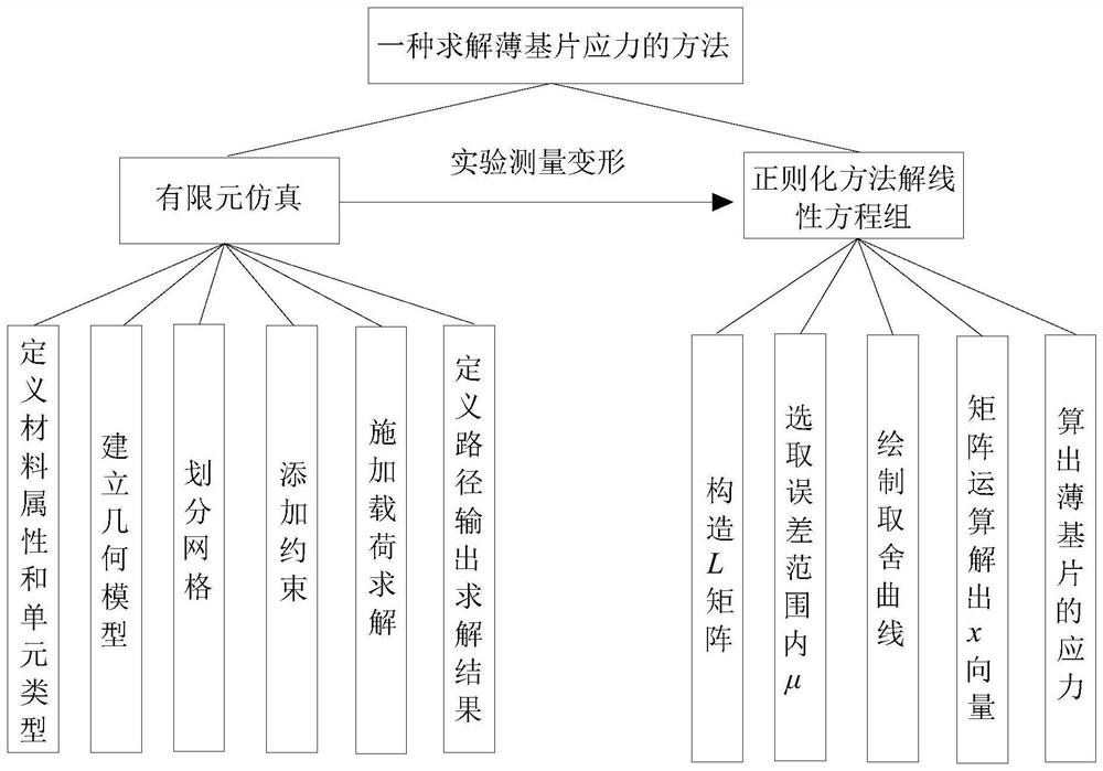
[0082] This embodiment provides a method for solving the stress of a thin substrate, such as figure 1 As shown, the technical solution can be summarized as two processes: finite element simulation and regularization method for solving linear equations.

[0083] The finite element simulation includes: defining material properties and element types, establishing geometric models, dividing meshes, adding constraints, applying loads to solve, and defining paths to output solution results. The regularization method to solve the linear equations includes: constructing an L matrix, selecting the penalty item coefficient μ of the regularization method, drawing a trade-off curve, matrix operation to solve the x vector, and calculating the relevant steps of the stress of the thin substrate.

[0084] In detail, the method provided in this embodiment includes the following steps:

[0085] S1: Obtain the basic parameters of the thin substrate to be analyzed for stress; the basic parameter...


PUM


Abstract

The invention belongs to the technical field of precision measurement and analysis, and particularly relates to a method for solving the stress of a thin substrate, which comprises the following steps of: S1, acquiring basic parameters of the thin substrate of which the stress is to be analyzed; S2, establishing a finite element model of the thin substrate; S3, applying a unit stress load to each surface in the model in sequence, solving the finite element model, and outputting a solving result; S4, obtaining the center point coordinates of the surfaces to which the unit stress load is applied in the finite element model, and further constructing a matrix L including the center point distance relationship between the surfaces; S5, acquiring the surface shape of the real thin substrate, and drawing an accept-reject curve; and S6, solving the linear equation by adopting a regularization method, and calculating to obtain the real stress distribution of the thin substrate. The problems of discontinuous stress distribution and large fluctuation of the thin substrate caused by directly solving the equation set are solved, and extra physical damage is not introduced in the process of obtaining the stress distribution.

Description

technical field [0001] The invention belongs to the technical field of precision measurement and analysis, and in particular relates to a method for solving the stress of a thin substrate. Background technique [0002] The thin substrate is a thin plate in mechanics, the geometric feature is circular, and its thickness dimension is much smaller than the plane dimension. At present, large-size silicon wafers of 300mm are widely used, and their thickness is less than 0.2mm. Due to the difference in temperature between the upper and lower surfaces during processing, residual stress will be generated on the surface of the silicon wafer after processing. Residual stress will lead to subsurface damage, the greater the damage, the greater the residual stress, so the residual stress can be used to characterize the damage of the silicon wafer subsurface. At present, in practical applications, laser triangulation and laser interferometers can be used to complete the measurement of t...

Claims


Application Information

Patent Timeline
IPC IPC(8): G06F30/23G06F119/14G06F111/04
CPCG06F30/23G06F2119/14G06F2111/04
Inventor 刘海军杨涛韩江夏链田晓青卢磊
Owner HEFEI UNIV OF TECH
Why Eureka
Try Eureka