Simulation and analysis method of link image quality based on full-band optical processing surface error system

A surface shape error and optical processing technology, which is applied in the direction of testing optical performance, adopting optical devices, design optimization/simulation, etc., to achieve the effects of improving imaging quality, shortening development cycle, and saving manufacturing costs

Active Publication Date: 2021-09-28
CHANGCHUN INST OF OPTICS FINE MECHANICS & PHYSICS CHINESE ACAD OF SCI
View PDF0 Cites 0 Cited by
  • Summary
  • Abstract
  • Description
  • Claims
  • Application Information

AI Technical Summary

Problems solved by technology

The analysis of the impact of full-band processing surface shape errors on parameters such as ellipticity and point spread function energy concentration in astronomy has not been reported yet.

Method used


Image

  • Simulation and analysis method of link image quality based on full-band optical processing surface error system
  • Simulation and analysis method of link image quality based on full-band optical processing surface error system
  • Simulation and analysis method of link image quality based on full-band optical processing surface error system

Examples


Embodiment Construction

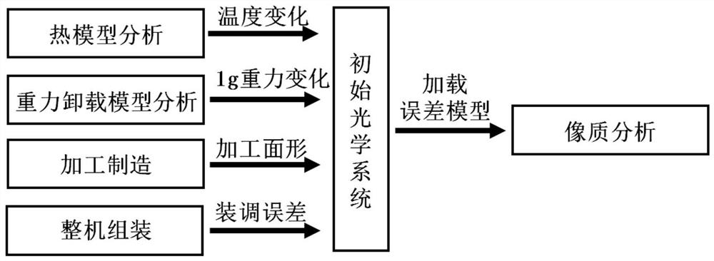
[0023] combine Figure 1 to Figure 11 Description of this embodiment, based on the full-band optical processing surface shape error system link image quality simulation analysis method, the method is implemented by the following steps:

[0024] Step 1. Complete the initial optical system design;

[0025] Complete the initial optical system design according to the use requirements, and assign parameters such as optics, mechanics, and electricity; then optimize the model of the optical system to make the parameters of the system meet the index requirements.

[0026] Step 2, establishing a simulation model of low-frequency error of the processed surface shape;

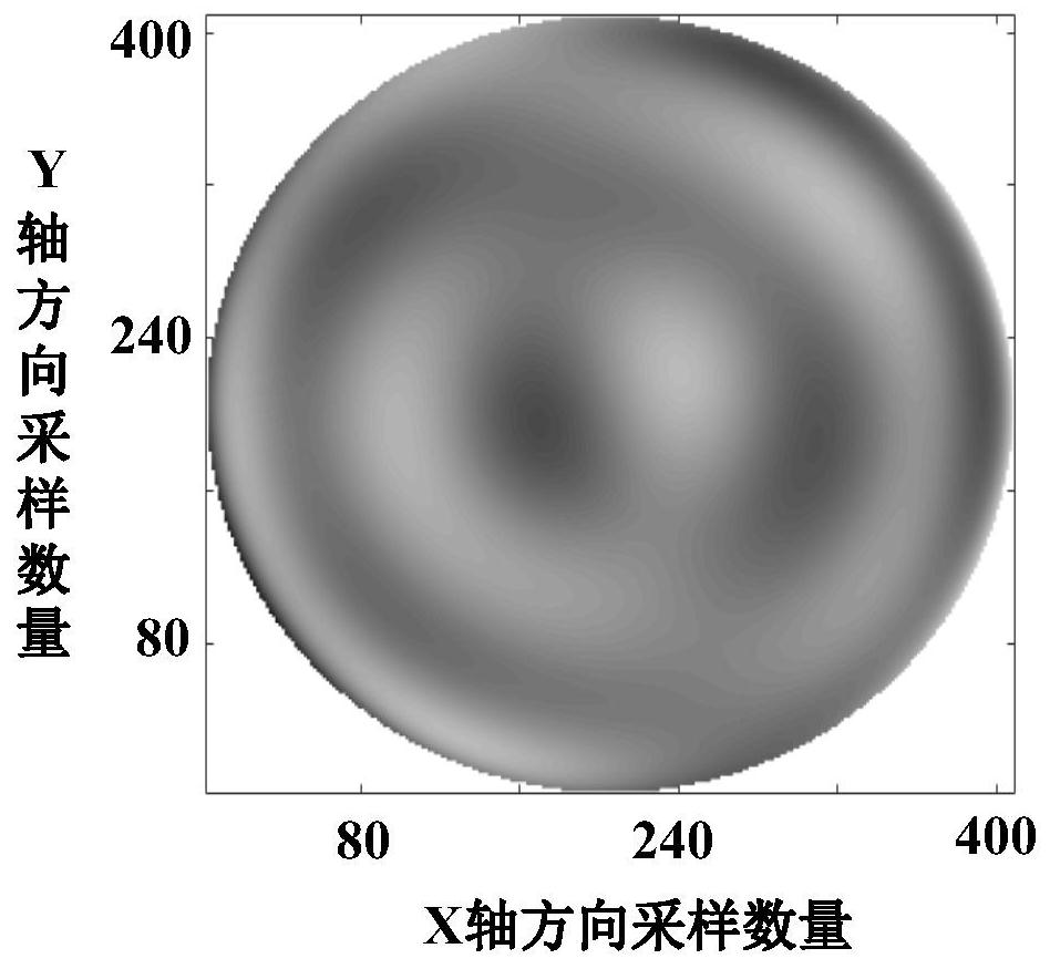
[0027] According to the previous processing surface shape data of optical components, the simulation of the processing surface shape is carried out. The low frequency part is obtained by fitting the first 37 Zernike polynomials.

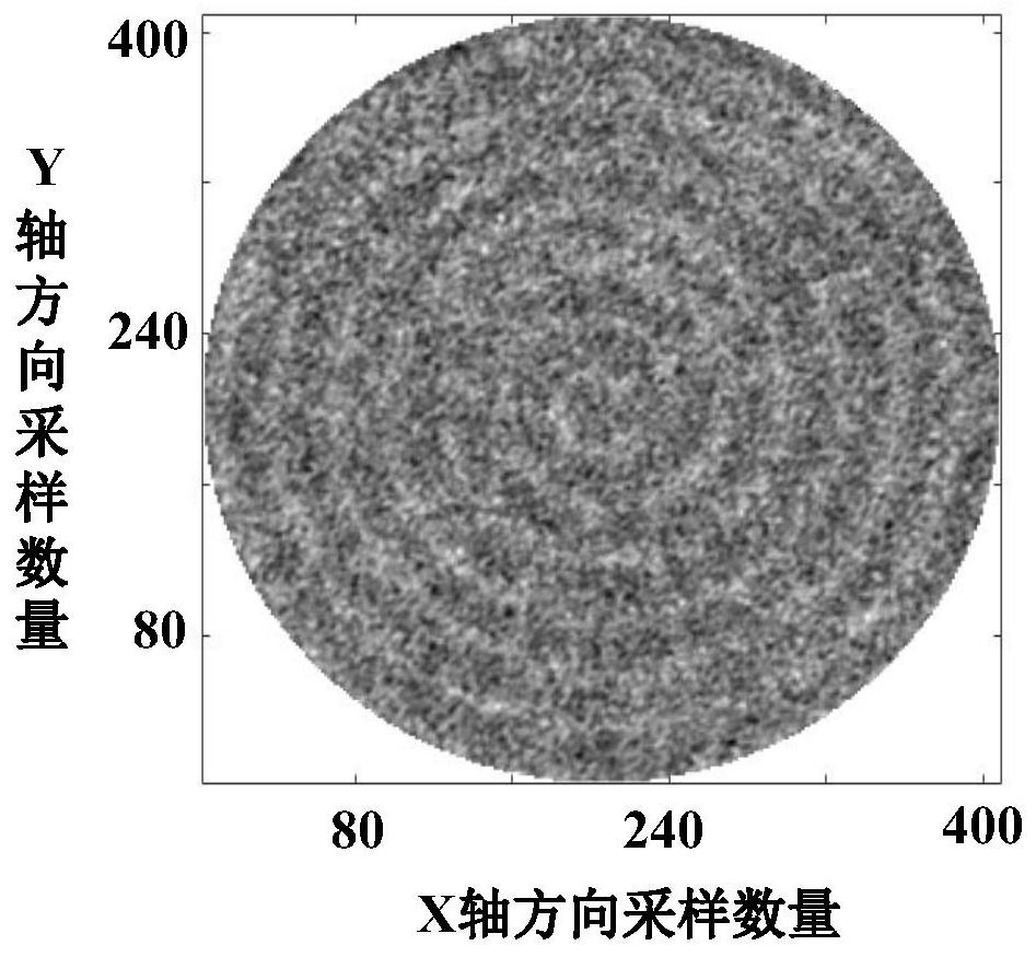
[0028] Step 3, establishing a simulation model of high-frequency errors in the processed ...


PUM


Abstract

Based on the image quality simulation analysis method of the full-band optical processing surface shape error system link, it relates to the field of photoelectric imaging technology. The present invention designs the optical system structure according to the user index requirements, establishes the optical system link model, and processes the surface shape data based on the measured optical elements. , the low-frequency error simulation model and the medium-high frequency error simulation model of the mirror surface shape are established. The simulation data of low-frequency and medium-high frequency processing surface error are fused to establish a full-band optical component processing surface error simulation model, and the accuracy of the full-frequency optical component processing surface error simulation model is tested. After the data accuracy inspection is completed, the processed surface shape error data is loaded into the optical link simulation system for image quality analysis. The present invention sets a reasonable data sampling interval. Establish an accurate simulation model of processing surface shape error, which lays the foundation for high-precision, fast calculation optical system link image quality simulation analysis.

Description

technical field [0001] The invention relates to the technical field of optical system integration simulation, in particular to a system link image quality simulation analysis method based on full-band optical processing surface shape error. Background technique [0002] Astronomy has been an important driving force behind the development of advanced technologies such as highly sensitive detectors, high-precision sensors and super-mobile computers. Observing the microcosm and space requires sophisticated optical equipment. The optical system link simulation method calculates the imaging quality of the optical system based on the physical mechanism of imaging, and is used to analyze and study the influence of various error factors on the optical image quality. Compared with experimental test analysis, accurate simulation can effectively shorten the equipment development cycle and save manufacturing costs. The processing surface error of optical components is one of the key f...

Claims


Application Information

Patent Timeline
Patent Type & Authority Patents(China)
IPC IPC(8): G01B11/24G01M11/02G06F30/20
CPCG01B11/24G01M11/02G06F30/20
Inventor 班章杨勋李晓波姜禹希
Owner CHANGCHUN INST OF OPTICS FINE MECHANICS & PHYSICS CHINESE ACAD OF SCI
Why Eureka
Try Eureka